SLVSAQ8G February 2011 – September 2017 TPS65185
PRODUCTION DATA.
- 1 Features
- 2 Applications
- 3 Description
- 4 Revision History
- 5 Description (continued)
- 6 Pin Configuration and Functions
- 7 Specifications
-
8 Detailed Description
- 8.1 Overview
- 8.2 Functional Block Diagram
- 8.3
Feature Description
- 8.3.1 Wake-Up and Power-Up Sequencing
- 8.3.2 Dependencies Between Rails
- 8.3.3 Soft Start
- 8.3.4 Active Discharge
- 8.3.5 VPOS/VNEG Supply Tracking
- 8.3.6 V3P3 Power Switch
- 8.3.7 VCOM Adjustment
- 8.3.8 Fault Handling And Recovery
- 8.3.9 Power Good Pin
- 8.3.10 Interrupt Pin
- 8.3.11 Panel Temperature Monitoring
- 8.4 Device Functional Modes
- 8.5 Programming
- 8.6
Register Maps
- 8.6.1 Thermistor Readout (TMST_VALUE) Register (address = 0x00h) [reset = N/A]
- 8.6.2 Enable (ENABLE) Register (address = 0x01h) [reset = 0h]
- 8.6.3 Voltage Adjustment (VADJ) Register (address = 0x02h) [reset = 23h]
- 8.6.4 VCOM 1 (VCOM1) Register (address = 0x03h) [reset = 7Dh]
- 8.6.5 VCOM 2 (VCOM2) Register (address = 0x04h) [reset = 04h]
- 8.6.6 Interrupt Enable 1 (INT_EN1) Register (address = 0x05h) [reset = 7Fh]
- 8.6.7 Interrupt Enable 2 (INT_EN2) Register (address = 0x06h) [reset = FFh]
- 8.6.8 Interrupt 1 (INT1) Register (address = 0x07h) [reset = 0h]
- 8.6.9 Interrupt 2 (INT2) Register (address = 0x08h) [reset = N/A]
- 8.6.10 Power-Up Sequence 0 (UPSEQ0) Register (address = 0x09h) [reset = E4h]
- 8.6.11 Power-Up Sequence 1 (UPSEQ1) Register (address = 0x0Ah) [reset = 55h]
- 8.6.12 Power-Down Sequence 0 (DWNSEQ0) Register (address = 0x0Bh) [reset = 1Eh]
- 8.6.13 Power-Down Sequence 1 (DWNSEQ1) Register (address = 0x0Ch) [reset = E0h]
- 8.6.14 Thermistor 1 (TMST1) Register (address = 0x0Dh) [reset = 20h]
- 8.6.15 Thermistor 2 (TMST2) Register (address = 0x0Eh) [reset = 78h]
- 8.6.16 Power Good Status (PG) Register (address = 0x0Fh) [reset = 0h]
- 8.6.17 Revision and Version Control (REVID) Register (address = 0x10h) [reset = 45h]
- 9 Application and Implementation
- 10Power Supply Recommendations
- 11Layout
- 12Device and Documentation Support
- 13Mechanical, Packaging, and Orderable Information
Package Options
Mechanical Data (Package|Pins)
Thermal pad, mechanical data (Package|Pins)
Orderable Information
7 Specifications
7.1 Absolute Maximum Ratings
over operating free-air temperature range (unless otherwise noted) (1)(2)| MIN | MAX | UNIT | |||
|---|---|---|---|---|---|
| Input voltage at VIN(2), VIN_P, VIN3P3 | –0.3 | 7 | V | ||
| Ground pins to system ground | –0.3 | 0.3 | V | ||
| Voltage at SDA, SCL, WAKEUP, PWRUP, VCOM_CTRL, VDDH_FB, VEE_FB, PWR_GOOD, nINT | –0.3 | 3.6 | V | ||
| Voltage on VB, VB_SW, VPOS_IN, VPOS_DIS, VDDH_IN | –0.3 | 20 | V | ||
| VDDH_DIS | –0.3 | 30 | V | ||
| Voltage on VN, VEE_IN, VCOM_PWR, VNEG_DIS, VNEG_IN | –20 | 0.3 | V | ||
| Voltage from VIN_P to VN_SW | –0.3 | 30 | V | ||
| Voltage on VCOM_DIS | –5 | 0.3 | V | ||
| VEE_DIS | –30 | 0.3 | V | ||
| Peak output current | Internally limited | mA | |||
| Continuous total power dissipation | 2 | W | |||
| TJ | Operating junction temperature | –10 | 125 | °C | |
| TA | Operating ambient temperature(3) | –10 | 85 | °C | |
| Tstg | Storage temperature | –65 | 150 | °C | |
(1) Stresses beyond those listed under Absolute Maximum Ratings may cause permanent damage to the device. These are stress ratings only, and functional operation of the device at these or any other conditions beyond those indicated under Recommended Operating Conditions is not implied. Exposure to absolute maximum rated conditions for extended periods may affect device reliability.
(2) All voltage values are with respect to network ground terminal.
(3) It is recommended that copper plane in proper size on board be in contact with die thermal pad to dissipate heat efficiently. Thermal pad is electrically connected to PBKG, which is supposed to be tied to the output of buck-boost converter. Thus wide copper trace in the buck-boost output will help heat dissipated efficiently.
7.2 ESD Ratings
| VALUE | UNIT | |||
|---|---|---|---|---|
| V(ESD) | Electrostatic discharge | Human-body model (HBM), per ANSI/ESDA/JEDEC JS-001(1) | ±2000 | V |
| Charged-device model (CDM), per JEDEC specification JESD22-C101(2) | ±500 | |||
(1) JEDEC document JEP155 states that 500-V HBM allows safe manufacturing with a standard ESD control process.
(2) JEDEC document JEP157 states that 250-V CDM allows safe manufacturing with a standard ESD control process.
7.3 Recommended Operating Conditions
over operating free-air temperature range (unless otherwise noted)7.4 Thermal Information
| THERMAL METRIC(1) | TPS65185 | TPS651851 | UNIT | ||
|---|---|---|---|---|---|
| RGZ (VQFN) | RSL (VQFN) | RSL (VQFN) | |||
| 48 PINS | 48 PINS | 48 PINS | |||
| RθJA | Junction-to-ambient thermal resistance | 30 | 30 | 30 | °C/W |
| RθJC(top) | Junction-to-case (top) thermal resistance | 15.6 | 16.2 | 16.2 | °C/W |
| RθJB | Junction-to-board thermal resistance | 6.6 | 5.1 | 5.1 | °C/W |
| ψJT | Junction-to-top characterization parameter | 0.2 | 0.2 | 0.2 | °C/W |
| ψJB | Junction-to-board characterization parameter | 6.6 | 5.1 | 5.1 | °C/W |
| RθJC(bot) | Junction-to-case (bottom) thermal resistance | 0.9 | 0.9 | 0.9 | °C/W |
(1) For more information about traditional and new thermal metrics, see the Semiconductor and IC Package Thermal Metrics application report.
7.5 Electrical Characteristics
| PARAMETER | TEST CONDITIONS | MIN | TYP | MAX | UNIT | ||
|---|---|---|---|---|---|---|---|
| INPUT VOLTAGE | |||||||
| VIN | Input voltage range | 3 | 3.7 | 6 | V | ||
| VUVLO | Undervoltage lockout threshold | VIN falling | 2.9 | V | |||
| VHYS | Undervoltage lockout hysteresis | VIN rising | 400 | mV | |||
| INPUT CURRENT | |||||||
| IQ | Operating quiescent current into VIN | Device switching, no load | 5.5 | mA | |||
| ISTD | Operating quiescent current into VIN | Device in standby mode | 130 | µA | |||
| ISLEEP | Shutdown current | Device in sleep mode | 3.5 | 10 | µA | ||
| INTERNAL SUPPLIES | |||||||
| VINT_LDO | Internal supply | 2.7 | V | ||||
| CINT_LDO | Nominal output capacitor | Capacitor tolerance ±10% | 1 | 4.7 | µF | ||
| VREF | Internal supply | 2.25 | V | ||||
| CREF | Nominal output capacitor | Capacitor tolerance ±10% | 3.3 | 4.7 | µF | ||
| DCDC1 (POSITIVE BOOST REGULATOR) | |||||||
| VIN | Input voltage range | 3 | 3.7 | 6 | V | ||
| PG | Power good threshold | Fraction of nominal output voltage | 90% | ||||
| Power good time-out | Not tested in production | 50 | ms | ||||
| VOUT | Output voltage range | 16 | V | ||||
| DC set tolerance | –4.5% | 4.5% | |||||
| IOUT | Output current | 250 | mA | ||||
| RDS(ON) | MOSFET on resistance | VIN = 3.7 V | 350 | mΩ | |||
| ILIMIT | Switch current limit (TPS65185) | 1.5 | A | ||||
| Switch current limit (TPS651851) | 2.5 | ||||||
| Switch current accuracy | –30% | 30% | |||||
| fSW | Switching frequency | 1 | MHz | ||||
| LDCDC1 | Inductor | 2.2 | µH | ||||
| CDCDC1 | Nominal output capacitor | Capacitor tolerance ±10% | 1 | 2 × 4.7 | µF | ||
| ESR | Output capacitor ESR | 20 | mΩ | ||||
| DCDC2 (INVERTING BUCK-BOOST REGULATOR) | |||||||
| VIN | Input voltage range | 3 | 3.7 | 6 | V | ||
| PG | Power good threshold | Fraction of nominal output voltage | 90% | ||||
| Power good time-out | Not tested in production | 50 | ms | ||||
| VOUT | Output voltage range | –16 | V | ||||
| DC set tolerance | –4.5% | 4.5% | |||||
| IOUT | Output current | 250 | mA | ||||
| RDS(ON) | MOSFET on resistance | VIN = 3.7 V | 350 | mΩ | |||
| ILIMIT | Switch current limit | 1.5 | A | ||||
| Switch current accuracy | –30% | 30% | |||||
| LDCDC1 | Inductor | 4.7 | µH | ||||
| CDCDC1 | Nominal output capacitor | Capacitor tolerance ±10% | 1 | 3 × 4.7 | µF | ||
| ESR | Capacitor ESR | 20 | mΩ | ||||
| LDO1 (VPOS) | |||||||
| VPOS_IN | Input voltage range | 15.2 | 16 | 16.8 | V | ||
| PG | Power good threshold | Fraction of nominal output voltage | 90% | ||||
| Power good time-out | Not tested in production | 50 | ms | ||||
| VSET | Output voltage set value | VIN = 16 V, VSET[2:0] = 0x3h to 0x6h |
14.25 | 15 | V | ||
| VINTERVAL | Output voltage set resolution | VIN = 16 V | 250 | mV | |||
| VOUTTOL | Output tolerance | VSET = 15 V, ILOAD = 20 mA, 3 V ≤ VIN < 5.9 V | –1% | 1% | |||
| VDROPOUT | Dropout voltage | ILOAD = 120 mA | 250 | mV | |||
| VLOADREG | Load regulation – DC | ILOAD = 10% to 90% | 1% | ||||
| ILOAD | Load current range (TPS65185) | VIN ≥ 3 V | 120 | mA | |||
| Load current range (TPS651851) | 3 V ≤ VIN < 3.6 V | 150 | |||||
| VIN ≥ 3.6 V | 200 | ||||||
| ILIMIT | Output current limit (TPS65185) | VIN ≥ 3 V | 120 | mA | |||
| Output current limit (TPS651851) | 3 V ≤ VIN < 3.6 V | 150 | |||||
| VIN ≥ 3.6 V | 200 | ||||||
| RDIS | Discharge impedance to ground | Enabled when rail is disabled | 800 | 1000 | 1200 | Ω | |
| Mismatch to any other RDIS | –2% | 2% | |||||
| CLDO1 | Nominal output capacitor | Capacitor tolerance ±10% | 1 | 4.7 | µF | ||
| LDO2 (VNEG) | |||||||
| VNEG_IN | Input voltage range | 15.2 | 16 | 16.8 | V | ||
| PG | Power good threshold | Fraction of nominal output voltage | 90% | ||||
| Power good time-out | Not tested in production | 50 | ms | ||||
| VSET | Output voltage set value | VIN = –16 V VSET[2:0] = 0x3h to 0x6h |
–15 | –14.25 | V | ||
| VINTERVAL | Output voltage set resolution | VIN = –16 V | 250 | mV | |||
| VOUTTOL | Output tolerance | VSET = –15 V, ILOAD = –20 mA | –1% | 1% | |||
| VDROPOUT | Dropout voltage | ILOAD = 120 mA | 250 | mV | |||
| VLOADREG | Load regulation – DC | ILOAD = 10% to 90% | 1% | ||||
| ILOAD | Load current range | 3 V ≤ VIN < 3.6 V (TPS65185 and TPS651851) | 120 | mA | |||
| VIN ≥ 3.6 V (TPS65185 and TPS651851) | 200 | ||||||
| ILIMIT | Output current limit | 3 V ≤ VIN < 3.6 V (TPS65185) | 180 | mA | |||
| 3 V ≤ VIN < 3.6 V (TPS651851) | 158 | ||||||
| VIN ≥ 3.6 V (TPS65185 and TPS651851) | 200 | ||||||
| RDIS | Discharge impedance to ground | Enabled when rail is disabled | 800 | 1000 | 1200 | Ω | |
| Mismatch to any other RDIS | –2% | 2% | |||||
| TSS | Soft-start time | Not tested in production | 1 | ms | |||
| CLDO2 | Nominal output capacitor | Capacitor tolerance ±10% | 1 | 4.7 | µF | ||
| LD01 (POS) AND LDO2 (VNEG) TRACKING | |||||||
| VDIFF | Difference between VPOS and VNEG | VSET = ±15 V, ILOAD = ±20 mA, 0°C to 60°C ambient, 3 V ≤ VIN < 5.9 V |
–50 | 50 | mV | ||
| VCOM DRIVER | |||||||
| IVCOM | Drive current | 15 | mA | ||||
| VCOM | Allowed operating range | Outside this range VCOM is shut down and VCOMF interrupt is set | –5.5 | 1 | V | ||
| Accuracy | VCOM[8:0] = 0x07Dh (–1.25 V), VIN = 3.4 V to 4.2 V, no load |
–0.8% | 0.8% | ||||
| VCOM[8:0] = 0x07Dh (–1.25 V), VIN = 3 V to 6 V, no load |
–1.5% | 1.5% | |||||
| Output voltage range | –5.11 | 0 | V | ||||
| Resolution | 1LSB | 10 | mV | ||||
| Max number of EEPROM writes | VCOM calibration | 100 | |||||
| RIN | Input impedance, HiZ state | HiZ = 1 | 150 | MΩ | |||
| RDIS | Discharge impedance to ground | VCOM_CTRL = low, Hi-Z = 0 | 800 | 1000 | 1200 | Ω | |
| Mismatch to any other RDIS | –2% | 2% | |||||
| CVCOM | Nominal output capacitor | Capacitor tolerance ±10% | 3.3 | 4.7 | µF | ||
| CP1 (VDDH) CHARGE PUMP | |||||||
| VDDH_IN | Input voltage range | 15.2 | 16 | 16.8 | V | ||
| PG | Power good threshold | Fraction of nominal output voltage | 90% | ||||
| Power good time-out | Not tested in production | 50 | ms | ||||
| VFB | Feedback voltage | 0.998 | V | ||||
| Accuracy | ILOAD = 2 mA | –2% | 2% | ||||
| VDDH_OUT | Output voltage range | VSET = 22 V, ILOAD = 2 mA, R6 = 1MΩ, R10 = 47.5 kΩ | 21 | 22 | 23 | V | |
| VSET = 25 V, ILOAD = 2 mA, R6 = 1MΩ, R10 = 41.6 kΩ | 24 | 25 | 26 | ||||
| VSET = 28 V, ILOAD = 2 mA, R6 = 1MΩ, R10 = 37 kΩ | 27 | 28 | 29 | ||||
| ILOAD | Load current range (TPS65185) | 10 | mA | ||||
| Load current range (TPS651851) | 15 | ||||||
| fSW | Switching frequency | 560 | kHz | ||||
| RDIS | Discharge impedance to ground | Enabled when rail is disabled | 800 | 1000 | 1200 | Ω | |
| Mismatch to any other RDIS | –2% | 2% | |||||
| CD | Driver capacitor | 10 | nF | ||||
| CO | Output capacitor | 1 | 2.2 | µF | |||
| CP2 (VEE) NEGATIVE CHARGE PUMP | |||||||
| VEE_IN | Input voltage range | 15.2 | 16 | 16.8 | V | ||
| PG | Power good threshold | Fraction of nominal output voltage | 90% | ||||
| Power good time-out | Not tested in production | 50 | ms | ||||
| VFB | Feedback voltage | –0.994 | V | ||||
| Accuracy | ILOAD = 2 mA | –2% | 2% | ||||
| VEE_OUT | Output voltage range | VSET = –20 V, ILOAD = 3 mA | –21 | –20 | –19 | V | |
| ILOAD | Load current range (TPS65185) | 12 | mA | ||||
| Load current range (TPS651851) | 15 | ||||||
| fSW | Switching frequency | 560 | kHz | ||||
| RDIS | Discharge impedance to ground | Enabled when rail is disabled | 800 | 1000 | 1200 | Ω | |
| Mismatch to any other RDIS | –2% | 2% | |||||
| CD | Driver capacitor | 10 | nF | ||||
| CO | Nominal output capacitor | Capacitor tolerance ±10% | 1 | 2.2 | µF | ||
| THERMISTOR MONITOR(1) | |||||||
| ATMS | Temperature to voltage ratio | Not tested in production | –0.0161 | V/°C | |||
| OffsetTMS | Offset | Temperature = 0°C | 1.575 | V | |||
| VTMS_HOT | Temp hot trip voltage (T = 50°C) | TEMP_HOT_SET = 0x8C | 0.768 | V | |||
| VTMS_COOL | Temp hot escape voltage (T = 45°C) | TEMP_COOL_SET = 0x82 | 0.845 | V | |||
| VTMS_MAX | Maximum input level | 2.25 | V | ||||
| RNTC_PU | Internal pullup resistor | 7.307 | kΩ | ||||
| RLINEAR | External linearization resistor | 43 | kΩ | ||||
| ADCRES | ADC resolution | Not tested in production, 1 bit | 16.1 | mV | |||
| ADCDEL | ADC conversion time | Not tested in production | 19 | µs | |||
| TMSTTOL | Accuracy | Not tested in production | –1 | 1 | LSB | ||
| LOGIC LEVELS AND TIMING CHARTERISTICS (SCL, SDA, PWR_GOOD, PWRx, WAKEUP) | |||||||
| VOL | Output low threshold level | IO = 3 mA, sink current (SDA, nINT, PWR_GOOD) |
0.4 | V | |||
| VIL | Input low threshold level | 0.4 | V | ||||
| VIH | Input high threshold level | 1.2 | V | ||||
| I(bias) | Input bias current | VIO = 1.8 V | 1 | µA | |||
| tdeglitch | Deglitch time, WAKEUP pin | Not tested in production | 500 | µs | |||
| Deglitch time, PWRUP pin | Not tested in production | 400 | |||||
| tdischarge | Discharge delay | Not tested in production | 100(2) | ms | |||
| fSCL | SCL clock frequency | 400 | kHz | ||||
| I2C slave address | 7-bit address | 0 × 68h(3) | |||||
| OSCILLATOR | |||||||
| fOSC | Oscillator frequency | 9 | MHz | ||||
| Frequency accuracy | TA = –40°C to 85°C | –10% | 10% | ||||
| THERMAL SHUTDOWN | |||||||
| TSHTDWN | Thermal trip point | 150 | °C | ||||
| Thermal hysteresis | 20 | °C | |||||
(1) 10-kΩ Murata NCP18XH103F03RB thermistor (1%) in parallel with a linearization resistor (43 kΩ, 1%) are used at TS pin for panel temperature measurement.
(2) Contact factory for 50-ms, 200-ms or 400-ms option.
(3) Contact TI for alternate address of 0 × 48h.
7.6 Timing Requirements: Data Transmission
VBAT = 3.6 V ±5%, TA = 25ºC, CL = 100 pF (unless otherwise noted)| MIN | NOM | MAX | UNIT | |||
|---|---|---|---|---|---|---|
| f(SCL) | Serial clock frequency | 100 | 400 | kHz | ||
| tHD;STA | Hold time (repeated) START condition. After this period, the first clock pulse is generated. | SCL = 100 kHz | 4 | µs | ||
| SCL = 400 kHz | 600 | ns | ||||
| tLOW | LOW period of the SCL clock | SCL = 100 kHz | 4.7 | µs | ||
| SCL = 400 kHz | 1.3 | |||||
| tHIGH | HIGH period of the SCL clock | SCL = 100 kHz | 4 | µs | ||
| SCL = 400 kHz | 600 | ns | ||||
| tSU;STA | Set-up time for a repeated START condition | SCL = 100 kHz | 4.7 | µs | ||
| SCL = 400 kHz | 600 | ns | ||||
| tHD;DAT | Data hold time | SCL = 100 kHz | 0 | 3.45 | µs | |
| SCL = 400 kHz | 0 | 900 | ns | |||
| tSU;DAT | Data set-up time | SCL = 100 kHz | 250 | ns | ||
| SCL = 400 kHz | 100 | |||||
| tr | Rise time of both SDA and SCL signals | SCL = 100 kHz | 1000 | ns | ||
| SCL = 400 kHz | 300 | |||||
| tf | Fall time of both SDA and SCL signals | SCL = 100 kHz | 300 | ns | ||
| SCL = 400 kHz | 300 | |||||
| tSU;STO | Set-up time for STOP condition | SCL = 100 kHz | 4 | µs | ||
| SCL = 400 kHz | 600 | ns | ||||
| tBUF | Bus Free Time Between Stop and Start Condition | SCL = 100 kHz | 4.7 | µs | ||
| SCL = 400 kHz | 1.3 | |||||
| tSP | Pulse width of spikes that must be suppressed by the input filter | SCL = 100 kHz | n/a | n/a | ns | |
| SCL = 400 kHz | 0 | 50 | ||||
| Cb | Capacitive load for each bus line | SCL = 100 kHz | 400 | pF | ||
| SCL = 400 kHz | 400 | |||||
 Figure 1. I2C Data Transmission Timing
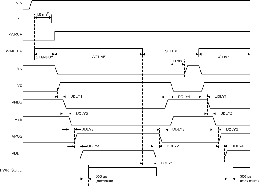
1. Minimum delay time between WAKEUP rising edge and IC ready to accept I2C transaction.
2. The device does not enter the SLEEP state until the final discharge delay time has elapsed.
NOTE:
In this example, the first power-up sequence is started by pulling the PWRUP pin high (rising edge). Power-down is initiated by pulling the WAKEUP pin low (device enters sleep mode after rails are discharged). The second power-up sequence is initiated by pulling the WAKEUP pin high while the PWRUP pin is also high (power up from sleep to active).7.7 Typical Characteristics
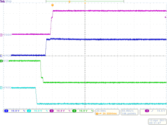
| VIN = 3.7 V | CIN = 100 µF | |
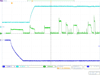
| VIN = 3 V | RLOAD, VPOS = 330 Ω | RLOAD, VNEG = 330 Ω |
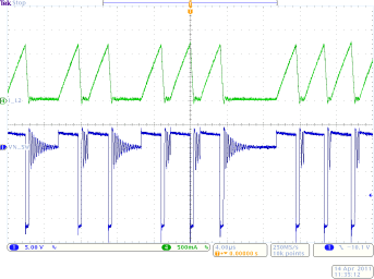
| No Load on VDDH, VEE | ||
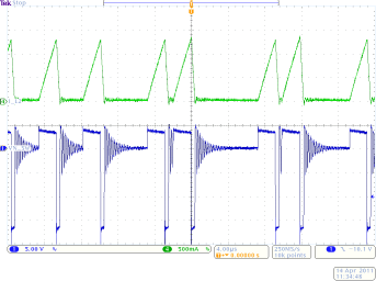
| VIN = 3.7 V | RLOAD, VPOS = 330 Ω | RLOAD, VNEG = 330 Ω |
| No Load on VDDH, VEE | ||

| VIN = 5 V | RLOAD, VPOS = 330 Ω | RLOAD, VNEG = 330 Ω |
| No Load on VDDH, VEE | ||
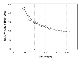
| VIN = 3.7 V | ILOAD, V3p3 = 10 mA | |
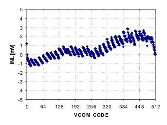
| VIN = 3.7 V | RLOAD, VCOM = 1 kΩ | |
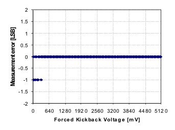
| VIN = 3.7 V | ||
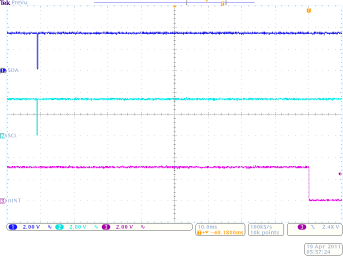
| VIN = 3.7 V | AVG[1:0] = 11 (Eight Measurements) | |
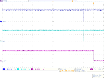
| Time from ACQ Bit Set to ACQC Interrupt Received | ||
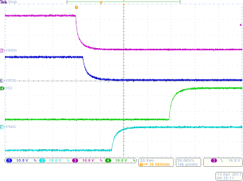
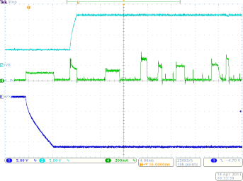
| VIN = 5 V | CIN = 100 µF | |
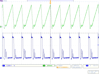
| VIN = 3 V | RLOAD, VPOS = 330 Ω | RLOAD, VNEG = 330 Ω |
| No Load on VDDH, VEE | ||
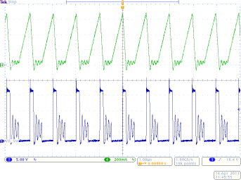
| VIN = 3.7 V | RLOAD, VPOS = 330 Ω | RLOAD, VNEG = 330 Ω |
| No Load on VDDH, VEE | ||
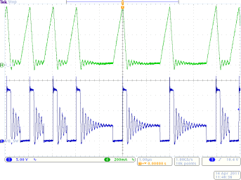
| VIN = 5 V | RLOAD, VPOS = 330 Ω | RLOAD, VNEG = 330 Ω |
| No Load on VDDH, VEE | ||
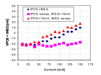
| VIN = 3.7 V | ||
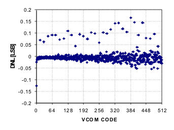
| VIN = 3.7 V | RLOAD, VCOM = 1 kΩ | |
| VIN = 3.7 V | AVG[1:0] = 00 (Single Measurement) | |
| Time from ACQ Bit Set to ACQC Interrupt Received | ||