SLVSBB0D April 2012 – February 2018 TPS65197
PRODUCTION DATA.
- 1 Features
- 2 Applications
- 3 Description
- 4 Revision History
- 5 Pin Configuration and Functions
- 6 Specifications
- 7 Detailed Description
- 8 Application and Implementation
- 9 Power Supply Recommendations
- 10Layout
- 11Device and Documentation Support
- 12Mechanical, Packaging, and Orderable Information
Package Options
Mechanical Data (Package|Pins)
- RUY|28
Thermal pad, mechanical data (Package|Pins)
Orderable Information
7.4.2 Charge-Sharing Methods TPS65197
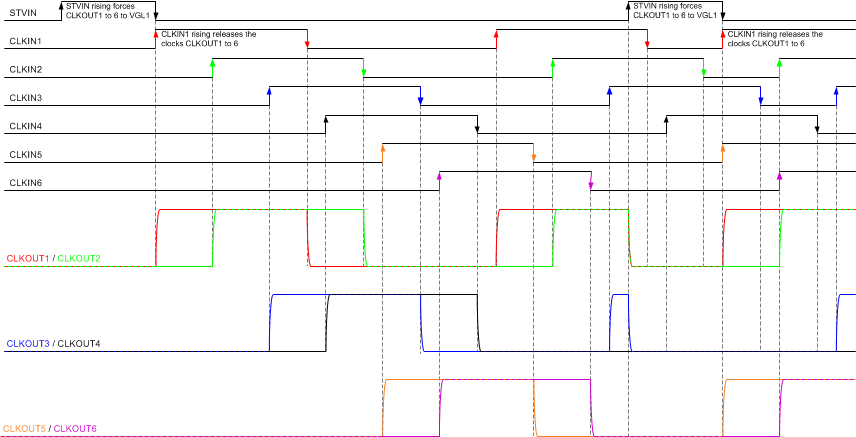
 Figure 4. TPS65197: Charge-Sharing Disabled (CS_SEL < 0.5 V)
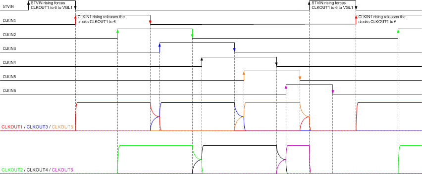
Charge-sharing of CLKOUT1 ↔ CLKOUT3 between CLKIN1↓ CLKIN3↑.
Charge-sharing of CLKOUT3 ↔ CLKOUT5 between CLKIN3↓ CLKIN5↑.
Charge-sharing of CLKOUT5 ↔ CLKOUT1 between CLKIN5↓ CLKIN1↑.
Charge-sharing of CLKOUT2 ↔ CLKOUT4 between CLKIN2↓ CLKIN4↑.
Charge-sharing of CLKOUT4 ↔ CLKOUT6 between CLKIN4↓ CLKIN6↑.
Charge-sharing of CLKOUT6 ↔ CLKOUT2 between CLKIN6↓ CLKIN2↑.
Figure 5. TPS65197: 3-Channel Charge-Sharing (CS_SEL = 1 V…2 V)Charge-sharing of CLKOUT3 ↔ CLKOUT5 between CLKIN3↓ CLKIN5↑.
Charge-sharing of CLKOUT5 ↔ CLKOUT1 between CLKIN5↓ CLKIN1↑.
Charge-sharing of CLKOUT2 ↔ CLKOUT4 between CLKIN2↓ CLKIN4↑.
Charge-sharing of CLKOUT4 ↔ CLKOUT6 between CLKIN4↓ CLKIN6↑.
Charge-sharing of CLKOUT6 ↔ CLKOUT2 between CLKIN6↓ CLKIN2↑.

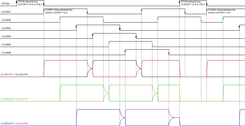
Charge-sharing of CLKOUT1 ↔ CLKOUT4 between CLKIN1↓ CLKIN4↑ and CLKIN4↓ CLKIN1↑.
Charge-Sharing of CLKOUT2 ↔ CLKOUT5 between CLKIN2↓ CLKIN5↑ and CLKIN5↓ CLKIN2↑.
Charge-Sharing of CLKOUT3 ↔ CLKOUT6 between CLKIN3↓ CLKIN6↑ and CLKIN6↓ CLKIN3↑.
Figure 6. TPS65197: 2-Channel Charge-Sharing (CS_SEL = 2.8 V…6.5 V)Charge-Sharing of CLKOUT2 ↔ CLKOUT5 between CLKIN2↓ CLKIN5↑ and CLKIN5↓ CLKIN2↑.
Charge-Sharing of CLKOUT3 ↔ CLKOUT6 between CLKIN3↓ CLKIN6↑ and CLKIN6↓ CLKIN3↑.