SLVSBB0D April 2012 – February 2018 TPS65197
PRODUCTION DATA.
- 1 Features
- 2 Applications
- 3 Description
- 4 Revision History
- 5 Pin Configuration and Functions
- 6 Specifications
- 7 Detailed Description
- 8 Application and Implementation
- 9 Power Supply Recommendations
- 10Layout
- 11Device and Documentation Support
- 12Mechanical, Packaging, and Orderable Information
Package Options
Mechanical Data (Package|Pins)
- RUY|28
Thermal pad, mechanical data (Package|Pins)
Orderable Information
3 Description
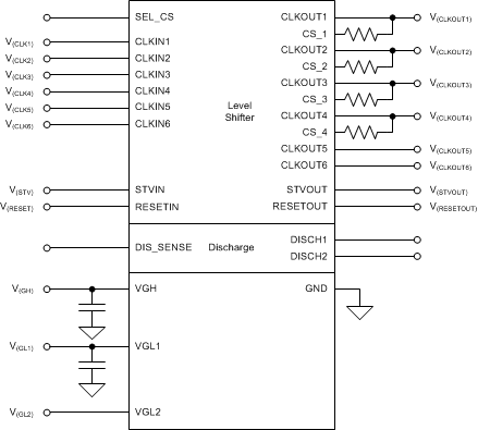
The TPS65197/B is an 8-channel level-shifter with discharge function intended for use in LCD display applications such as Notebooks, Monitors and TVs.
The device converts the timing-controller (T-CON) logic-level signals to the high-level signals needed by the gate-in-panel (GIP) display.
The clock outputs, CLKOUTx, support normal level shifting operation and 2-channel or 3-channel charge-sharing, which can be used to improve picture quality and power consumption. At power down, all outputs follow their input signals as long as possible; when the discharge function is used, the outputs are pulled high (VGH).
The TPS65197 implements a logic reset to ignore wrong T-CON signals after the rising STV edge which forces all 6 output clocks to VGL1. The next CLKIN1 rising edge unlocks the logic and enables normal operation. The TPS65197B does not have the logic reset and always follows its input signals.
Device Information(1)
| PART NUMBER | PACKAGE | BODY SIZE (NOM) |
|---|---|---|
| TPS65197 | WQFN (28) | 4.00 mm x 4.00 mm |
| TPS65197B | WQFN (28) | 4.00 mm x 4.00 mm |
- For all available packages, see the orderable addendum at the end of the datasheet.
