SLVSBB0D April 2012 – February 2018 TPS65197
PRODUCTION DATA.
- 1 Features
- 2 Applications
- 3 Description
- 4 Revision History
- 5 Pin Configuration and Functions
- 6 Specifications
- 7 Detailed Description
- 8 Application and Implementation
- 9 Power Supply Recommendations
- 10Layout
- 11Device and Documentation Support
- 12Mechanical, Packaging, and Orderable Information
Package Options
Mechanical Data (Package|Pins)
- RUY|28
Thermal pad, mechanical data (Package|Pins)
Orderable Information
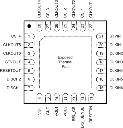
5 Pin Configuration and Functions
RUY Package
28-Pin WQFN With Thermal Pad
Top View

Pin Functions
| PIN | I/O/P | DESCRIPTION | |
|---|---|---|---|
| NAME | NUMBER | ||
| CLKIN1 | 20 | I | Clock 1 input |
| CLKIN2 | 19 | I | Clock 2 input |
| CLKIN3 | 18 | I | Clock 3 input |
| CLKIN4 | 17 | I | Clock 4 input |
| CLKIN5 | 16 | I | Clock 5 input |
| CLKIN6 | 15 | I | Clock 6 input |
| CLKOUT1 | 22 | I/O | Clock 1 output |
| CLKOUT2 | 24 | I/O | Clock 2 output |
| CLKOUT3 | 26 | I/O | Clock 3 output |
| CLKOUT4 | 28 | I/O | Clock 4 output |
| CLKOUT5 | 2 | I/O | Clock 5 output |
| CLKOUT6 | 3 | I/O | Clock 6 output |
| CS_1 | 23 | I/O | Clock 1 charge-sharing input |
| CS_2 | 25 | I/O | Clock 2 charge-sharing input |
| CS_3 | 27 | I/O | Clock 3 charge-sharing input |
| CS_4 | 1 | I/O | Clock 4 charge-sharing input |
| DISCH1 | 7 | I/O | Discharge 1 output. Internally connected to VGL1 and VGH |
| DISCH2 | 6 | I/O | Discharge 2 output. Internally connected to VGL2 and VGH |
| DIS_SENSE | 13 | I | Discharge sense terminal |
| GND | 9 | – | Ground |
| RESETIN | 14 | I | RESET input |
| RESETOUT | 5 | I/O | RESET output |
| SEL_CS | 12 | I | Charge-sharing method-selection terminal. When left floating or pulled to GND, charge-sharing is disabled. |
| STVIN | 21 | I | STV input |
| STVOUT | 4 | I/O | STV output |
| VGH | 8 | P | Positive supply voltage. Place a buffer capacitor close to this terminal. |
| VGL1 | 10 | P | Negative supply voltage for all outputs except discharge 2. Place a buffer capacitor close to this terminal. |
| VGL2 | 11 | P | Negative supply voltage for discharge 2 |
| Thermal pad | – | – | The thermal pad is connected to VGL1. |