SLVSBB0D April 2012 – February 2018 TPS65197
PRODUCTION DATA.
- 1 Features
- 2 Applications
- 3 Description
- 4 Revision History
- 5 Pin Configuration and Functions
- 6 Specifications
- 7 Detailed Description
- 8 Application and Implementation
- 9 Power Supply Recommendations
- 10Layout
- 11Device and Documentation Support
- 12Mechanical, Packaging, and Orderable Information
Package Options
Mechanical Data (Package|Pins)
- RUY|28
Thermal pad, mechanical data (Package|Pins)
Orderable Information
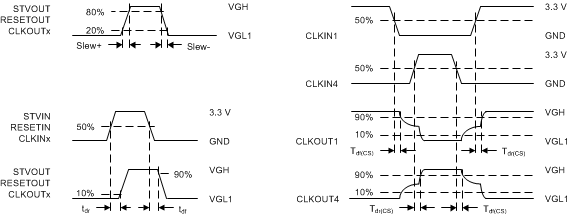
6.6 Switching Characteristics
over operating free-air temperature range (unless otherwise noted)| MIN | NOM | MAX | UNIT | |||
|---|---|---|---|---|---|---|
| LEVEL SHIFTERS (CLKOUT1 to CLKOUT6) | ||||||
| Slew+ | Slew rate, rising | C(OUT) = 4.7 nF, V(OUT) = 20% to 80% | 50 | 140 | V/µs | |
| Slew– | Slew rate, falling | 50 | 150 | |||
| tdr | Propagation delay | V(OUT) rising, C(OUT) = 150 pF | 40 | 100 | ns | |
| tdf | V(OUT) falling, C(OUT) = 150 pF | 50 | 100 | |||
| tdr(CS) | V(OUT) rising, C(OUT) = 150 pF, R(CS) = 50 Ω | 50 | 150 | |||
| tdf(CS) | V(OUT) falling, C(OUT) = 150 pF, R(CS) = 50 Ω | 70 | 150 | |||
| LEVEL SHIFTERS (STVOUT, RESETOUT) | ||||||
| Slew+ | Slew rate, rising | C(OUT) = 4.7 nF, V(OUT) = 20% to 80% | 20 | 50 | V/µs | |
| Slew– | Slew rate, falling | 30 | 60 | |||
| tdr | Propagation delay | V(OUT) rising, C(OUT) = 150 pF | 40 | 100 | ns | |
| tdf | V(OUT) falling, C(OUT) = 150 pF | 50 | 100 | |||
