SLVSA48A April 2010 – September 2015 TPS65200
PRODUCTION DATA.
- 1 Features
- 2 Applications
- 3 Description
- 4 Revision History
- 5 Pin Configuration and Functions
- 6 Specifications
-
7 Detailed Description
- 7.1 Overview
- 7.2 Functional Block Diagram
- 7.3 Feature Description
- 7.4
Device Functional Modes
- 7.4.1
Charge Mode Operation
- 7.4.1.1 Input Current Limiting and D+/D- Detection
- 7.4.1.2 Bad Adaptor Detection/Rejection (CHBADI)
- 7.4.1.3 Input Current Limiting at Start-Up
- 7.4.1.4 Charge Profile
- 7.4.1.5 Precharge to Fast Charge Threshold (VSHORT)
- 7.4.1.6 PWM Controller in Charge Mode
- 7.4.1.7 Battery Charging Process
- 7.4.1.8 Thermal Regulation and Protection
- 7.4.1.9 Safety Timer in Charge and Boost Mode (CH32MI, BST32SI)
- 7.4.1.10 Input Voltage Protection in Charge Mode
- 7.4.1.11 Battery Protection in Charge Mode
- 7.4.1.12 Charge Status Output, STAT Pin
- 7.4.2 Boost Mode Operation
- 7.4.3 High Impedance Mode
- 7.4.1
Charge Mode Operation
- 7.5 Programming
- 7.6
Register Maps
- 7.6.1 Control Register (CONTROL)
- 7.6.2 Charger Config Register A (CONFIG_A)
- 7.6.3 Charger Config Register B (CONFIG_B)
- 7.6.4 Charger Config Register C (CONFIG_C)
- 7.6.5 Charger Config Register D (CONFIG_D)
- 7.6.6 WLED Control Register (WLED)
- 7.6.7 Status Register A (STATUS_A)
- 7.6.8 Status Register B (STATUS_B)
- 7.6.9 Interrupt Register 1 (INT1)
- 7.6.10 Interrupt Register 2 (INT2)
- 7.6.11 Interrupt Register 3 (INT3)
- 7.6.12 Interrupt Mask Register 1 (MASK1)
- 7.6.13 Interrupt Mask Register 2 (MASK2)
- 7.6.14 Interrupt Mask Register 3 (MASK3)
- 7.6.15 Chip ID Register (CHIPID)
- 8 Application and Implementation
- 9 Power Supply Recommendations
- 10Layout
- 11Device and Documentation Support
- 12Mechanical, Packaging, and Orderable Information
Package Options
Mechanical Data (Package|Pins)
- YFF|36
Thermal pad, mechanical data (Package|Pins)
Orderable Information
7 Detailed Description
7.1 Overview
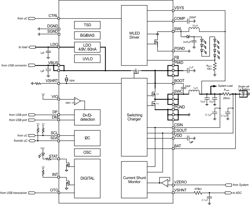
The TPS65200 charger features a synchronous 3-MHz PWM controller with integrated power MOSFETs, input current sensing and regulation, input-voltage dynamic power management, high-accuracy charge current and voltage regulation, and charge termination. The charger charges the battery in three phases: low-current precharge, constant current fast-charge, and constant voltage trickle-charge. The input current is automatically limited to the value set by the host. The charger can be configured to terminate charge based on user-selectable minimum current level and to automatically restart the charge cycle if the battery voltage falls below the recharge threshold. A safety timer with reset control provides a safety backup for I2C interface. The charger automatically enters sleep mode or high impedance mode when the input supply is removed. The charge status is reported to the host using the I2C interface and STAT pin. The D+D- detection circuit allows automatic detection of a USB wall-charger. If a wall-charger is detected the input current limit is automatically increased from 500 mA to 975 mA.
In OTG mode the PWM controller boosts the battery voltage to 5 V and provides up to 200-mA of current to the USB output. At very light loads the boost operates in burst mode to optimize efficiency. OTG mode can be enabled either through I2C interface or GPIO control.
The TPS65200 also provides a WLED boost converter with integrated 40-V switch FET, that drives up to 10 WLEDs in series. The boost converter runs at 600-kHz fixed switching frequency to reduce output ripple, improve conversion efficiency, and allows for the use of small external components. The default WLED current is set with a sense resistor, and the feedback voltage is regulated to 200 mV, as shown in the typical application. For brightness dimming, the feedback voltage can be changed through the I2C interface or by application of a PWM signal to the CTRL pin. In the latter case the feedback voltage is regulated down proportional to the PWM duty cycle (analog dimming) rather than pulsing the LED current to avoid audible noise on the output capacitor. For maximum protection, the device features integrated open LED protection that disables the TPS65200 to prevent the output from exceeding the absolute maximum ratings during open LED conditions.
A fixed-gain, high-accuracy current shunt monitor senses the voltage drop across an external, 20-mΩ sense resistor and provides an analog output voltage that is proportional to the charge/discharge current of the battery. The sense voltage is amplified by a factor of 25 and offset by VZERO, an externally provided reference voltage. VZERO is internally buffered to avoid loading of the reference source.
7.2 Functional Block Diagram
7.3 Feature Description
7.3.1 Global State Diagram
During normal operation, TPS65200 is either in STANDBY mode or ACTIVE mode, depending on user inputs. In STANDBY mode, most functions are turned off to conserve power, but the IC can still be accessed through I2C bus and the current shunt monitor can be turned on and off. The bias system and main oscillator are turned off in STANDBY mode.
The device enters ACTIVE mode whenever VBUS is asserted or the WLED driver is turned on. In ACTIVE mode, the main oscillator and reference system are turned on. The device remains in ACTIVE mode as long as VBUS remains high, the WLED driver is enabled or both conditions exist.
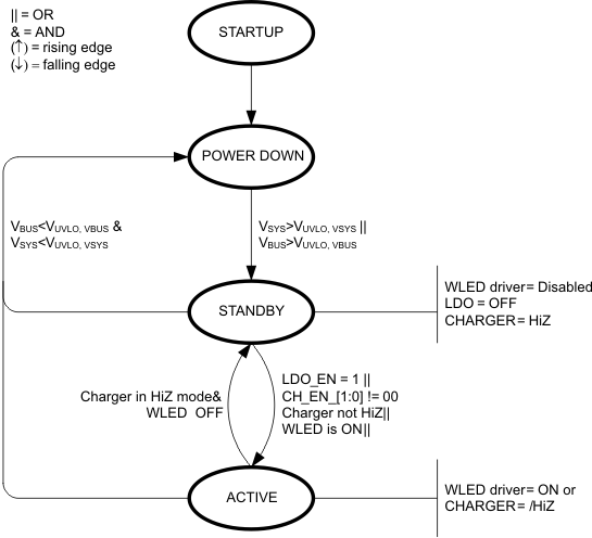 Figure 36. Global State Diagram
7.3.2 LED Driver Operation
The TPS65200 offers a high-efficiency, high-output voltage boost converter designed for driving up to 10 white LED in series. The serial LED connection provides even illumination by sourcing the same output current through all LEDs, eliminating the need for expensive factory calibration. The device integrates 40-V/0.7-A switch FET and operates in pulse width modulation (PWM) with 600-kHz fixed switching frequency. For operation, see Functional Block Diagram.
The LED driver can be enabled either through the CTRL pin or the WLED_EN bit in the CONTROL register. The CTRL input is edge sensitive and should be pulled low at power-up. The CTRL pin allows PWM dimming of the LEDs whereas the WLED_EN bit offers simple ON/OFF control only. The WLED_EN bit has priority over the CTRL pin and when set to 1, the CTRL pin is ignored. If WLED_EN is set to 0 and the CTRL pin is low for
> 2.5 ms, the WLED driver is shut down.
The feedback loop regulates the FB pin voltage to the reference set by the VFB[4:0] bits in the WLED register with a default setting of 200 mV. If any fault occurs during normal operation the driver is disabled, WLED_EN bit is reset to 0 and the driver is put into FAULT state until the CTRL pin has been low for > 2.5 ms. The state diagram for the WLED driver is shown in Figure 37.
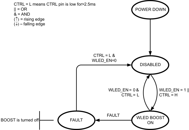 Figure 37. State Diagram for WLED Driver
7.3.2.1 Undervoltage Lockout
An undervoltage lockout circuit prevents operation of the WLED driver at input voltages (CSOUT pin) below 2.2 V. When the input voltage is below the under voltage threshold, the driver is shutdown and the internal switch FET is turned off. If the input voltage rises by 70 mV above the undervoltage lockout hysteresis, the WLED driver restarts. An internal thermal shutdown turns off the device when the typical junction temperature of 165°C is exceeded. The device is released from shutdown automatically when the junction temperature decreases by 10°C.
7.3.2.2 Shutdown
To minimize current consumption, the WLED driver is shutdown when the WLED_EN bit is low and the CTRL pin is pulled low for more than 2.5 ms. Although the internal FET does not switch in shutdown, there is still a DC current path between the input and the LEDs through the inductor and Schottky diode. The minimum forward voltage of the LED array must exceed the maximum input voltage to ensure that the LEDs remain off in shutdown. However, in the typical application with two or more LEDs, the forward voltage is large enough to reverse bias the Schottky and keep leakage current low.
7.3.2.3 Soft-Start Circuit
Soft-start circuitry is integrated into the WLED driver to avoid a high inrush current during start-up. After the device is enabled, the voltage at FB pin ramps up to the reference voltage in 32 steps, each step takes 213 µs. This ensures that the output voltage rises slowly to reduce the input current. Additionally, for the first 5 ms after the COMP voltage ramps, the current limit of the switch is set to half of the normal current limit specification. During this period, the input current is kept below 400 mA (typical).
7.3.2.4 Open LED Protection
Open LED protection circuitry prevents IC damage as the result of white LED disconnection. The TPS65200 monitors the voltage at the SWL pin during each switching cycle. The circuitry turns off the switch FET and shuts down the WLED driver as soon as the SWL voltage exceeds the VOVP threshold for eight clock cycles. As a result, the output voltage falls to the level of the input supply. The WLED driver remains in shutdown mode until it is enabled by toggling the CTRL pin or the WLED_EN bit of the CTRL register.
7.3.2.5 Current Program
The FB voltage is regulated to a low 200-mV reference voltage. The LED current is programmed externally using a current-sense resistor in series with the LED string. The value of the RSET is calculated using Equation 1.

where
- ILED = output current of LEDs
- VFB = regulated voltage of FB
- RSET = current sense resistor
The output current tolerance depends on the FB accuracy and the current sensor resistor accuracy.
7.3.2.6 Brightness Dimming
The TPS65200 offers two methods of LED brightness dimming. When the CTRL pin is constantly high, the FB voltage is regulated to the value set in the WLED register which ranges from 0 mV to 200 mV and is divided into 32 steps. For applications requiring higher dimming resolution, a PWM signal can be applied to the CTRL pin to reduce this regulation voltage and dim LED brightness. The relationship between the duty cycle and FB voltage is given by Equation 2.

where
- Duty = duty cycle of the PWM signal
- VFB[4:0] = internal reference voltage, default = 200 mV
The IC chops up the internal reference voltage at the duty cycle of the PWM signal and filters it by an internal low pass filter. The output of the filter is connected to the error amplifier as the reference voltage for the FB pin regulation. Therefore, although a PWM signal is used for brightness dimming, only the WLED DC current is modulated, which is often referred to as analog dimming. This eliminates the audible noise which often occurs when the LED current is pulsed in replica of the frequency and duty cycle of PWM control. The regulation voltage itself is independent of the PWM logic voltage level which often has large variations.
 Figure 38. WLED Analog Dimming Circuit
7.3.2.7 Inductor Overcurrent Protection
The overcurrent limit in the boost converter limits the maximum input current and thus maximum input power for a given input voltage. Maximum output power is less than maximum input power due to power conversion losses. Therefore, the current limit setting, input voltage, output voltage and efficiency can all change maximum current output. The current limit clamps the peak inductor current and the maximum DC output current equals the current limit minus half of the peak-peak current ripple. The ripple current is a function of switching frequency, inductor value and duty cycle. Equation 3 through Equation 5 are used to determine the maximum output current.

where
- D = duty cycle of the boost converter
- VIN = Input voltage
- VOUT = Output voltage of the boost converter. It is equal to the sum of VFB and the voltage drop across LEDs.

where
- IPP = inductor peak to peak ripple
- L = inductor value
- fs = switching frequency

where
- IOUT(MAX) = maximum output current of the boost converter
- ILIM = overcurrent limit
- η = efficiency
For instance, for VIN = 3 V, 7 LEDs output equivalent to VOUT of 23 V, an inductor value of 22 µH, a current limit of 700 mA, and an efficiency of 85%, the maximum output current is ~65 mA.
7.3.3 HV LDO
TPS65200 provides a 4.9-V LDO that is powered off the VBUS input. The LDO is enabled whenever VVBUS > VUVLO (3.3 V) and disabled when VVBUS > VOVP-IN_USB (6.5 V). LDO output voltage follows VBUS for VVBUS < 4.9 V and is regulated to 4.9 V when VVBUS > 4.9 V. In any case output current is limited to 100 mA. The LDO can also be disabled by the host by setting the LDO_EN bit of the CONTROL register to 0. An operational flow chart of the LDO enable is shown in Figure 39.
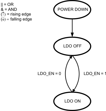 Figure 39. State Diagram for the HV LDO
7.3.4 Interrupt Pin
The interrupt pin is used to signal any fault condition to the host processor. Whenever a fault occurs in the IC, the corresponding fault bit is set in the INT1, INT2, or INT3 register, and the open-drain output is pulled low. The INT pin is released (returns to HiZ state) if any of the INT1, INT2, INT3 registers is accessed by the host, but fault bits are cleared only by reading the INTx register containing the bit. However, if a failure persists, the corresponding interrupt bit remains set but no new interrupt is issued. The TSD bit (thermal shutdown) is auto cleared which means that the bit is reset to 0 automatically after the chip has cooled down below the thermal shutdown release threshold.
The MASK1, MASK2, and MASK3 registers are used to mask certain events or group of events from generating interrupts. The MASKx settings affect the INT pin only and have no impact on protection and monitor circuits themselves.
7.3.5 Current Shunt Monitor
TPS65230 offers an integrated high-precision current shunt monitor to measure battery charging and discharging currents. The inputs of a low-offset amplifier are connected across an external low-value shunt resistor. This shunt voltage is gained up by a factor of 25 and added to a reference voltage connected to the VZERO terminal.
VSHUNT > VZERO for currents flowing into the battery and VSHUNT < VZERO for currents flowing out of the battery. The reference voltage is buffered by a low-offset, high impedance input buffer.

where
- VSHUNT is the output voltage of the current shunt monitor
- VCSIN is the charger side of the shunt resistor
- VCSOUT is the battery side of the shunt resistor
- VZERO is the 0-current reference voltage
- VOFFSET is the offset of the differential amplifier
The offset of the differential amplifier introduces a measurement error of ±40 µV input referred, equivalent to ±2 mA assuming a 20-mΩ shunt resistor which can be calibrated out by the system.
The shunt monitor is disabled by default and can be enabled by the host by setting the SMON_EN bit in the CONTROL register to 1.
7.4 Device Functional Modes
7.4.1 Charge Mode Operation
For current limited power source, such as a USB host or hub, the high efficiency converter is critical in fully utilizing the input power capacity and quickly charging the battery. Due to the high efficiency in a wide range of the input voltage and battery voltage, the switching mode charger is a good choice for high speed charging with less power loss and better thermal management.
The TPS65200 is a highly-integrated synchronous switched-mode charger with reverse boost function for USB OTG support, featuring integrated MOSFETs and small external components, targeted at extremely space-limited portable applications powered by 1-cell Li-ion or Li-polymer battery pack.
 Figure 40. State Diagram of USB Charger Circuit
The TPS65200 has three operation modes: charge mode, boost mode, and high impedance mode. In charge mode, the TPS65200 supports a precision Li-ion or Li-polymer charging system for single-cell applications. In boost mode, TPS65200 will boost the battery voltage to VBUS for powering attached OTG devices. In high impedance mode, the TPS65200 charger stops charging or boosting and operates in a mode with very low current from VBUS or battery, to effectively reduce the power consumption when the portable device is in standby mode. Through carefully designed internal control circuits, TPS65200 achieves smooth transition between different operation modes.
The global state diagram of the charger is shown in Figure 40 and the detailed charging algorithm in Figure 41. HiZ mode is the default state of the charger where Q1, charger PWM and boost operation is turned off. If any fault occurs during charging, the CH_EN[1:0] bits in the CONTROL register are reset to 00b (OFF), fault bits are set in the INT2 register, an interrupt is issued on the INT pin, and HiZ mode is entered. Charging is re-initiated by either host control or automatically if VBUS is power cycled.
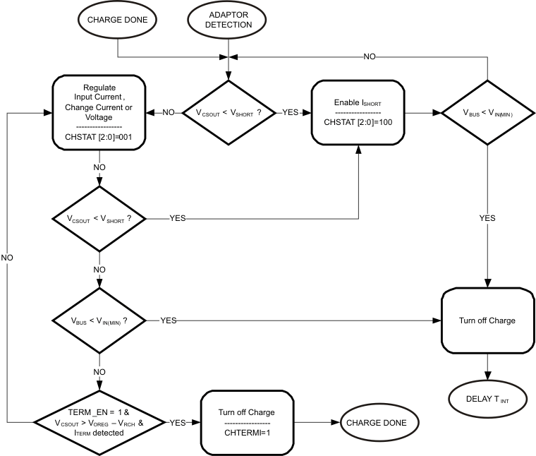 Figure 41. Detailed Charging Flow Chart
7.4.1.1 Input Current Limiting and D+/D- Detection
By default the VBUS input current limit is set to 500 mA. When VBUS is asserted the TPS65200 performs a charger source identification to determine if it is connected to a USB port or dedicated charger. This detection is performed 200 ms after VBUS is asserted to ensure the USB plug has been fully inserted before identification is performed. If a dedicated charger is detected the input current limit is increased to 975 mA, otherwise the current limit remains at 500 mA, unless changed by the user.
Automatic detection is performed only if VIO is below 0.6 V to avoid interfering with the USB transceiver which may also perform D+/D- detection when the system is running normally. However, D+/D- can be initiated at any time by the host by setting the DPDM_EN bit in the CONTROL register to 1. After detection is complete the DPDM_EN bit is automatically reset to 0 and the detection circuitry is disconnected from the DP DM pins to avoid interference with USB data transfer.
The input current limit can also be set through the I2C interface to 100 mA, 500 mA, 975 mA, or no limit by writing to the CONFIG_B register. The effective current limit will be the higher of the D+D- detection result and the IIN_LIMIT[1:0] setting in CONFIG_A register. Whenever VBUS drops below the UVLO threshold IIN_LIMIT[1:0] is reset to 100-mA setting to avoid excessive current draw from an unknown USB port.
Once the input current reaches the input current limiting threshold, the charge current is reduced to keep the input current from exceeding the programmed threshold. The host can choose to ignore the D+D- detection result by setting the LMTSEL bit of the CONFIG_A register to 1.
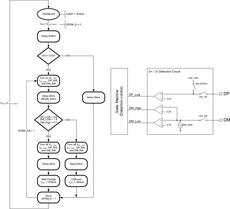 Figure 42. Adaptor Identification Algorithm and Block Diagram
7.4.1.2 Bad Adaptor Detection/Rejection (CHBADI)
At the beginning of the charge cycle, the IC will perform the bad adaptor detection by applying a current sink to VBUS. If VVBUS is higher than VIN(MIN) for 30 ms, the adaptor is good and the charge process will begin. However, if VVBUS drops below VIN(MIN), a bad adaptor is detected. Then, the IC will disable the current sink, issue an interrupt and set the CHBADI interrupt in the INT2 register. After a delay of TINT (2s), the IC will repeat the adaptor detection process, as shown in Figure 44.
If the battery voltage is high (> 3.8 V), it is possible that the input voltage drops below the battery voltage during adaptor rejection test. In this case, the reverse protection will kick-in and disable the charger. Also note that the 30-mA current sink is turned on for 30 ms only. If the input capacitance is > 500 µF (not recommended), the adaptor may be accepted although it is not capable of providing 30-mA of current. In these cases, the VDPPM loop will limit the charging current to maintain the input voltage.
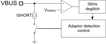 Figure 43. Bad Adaptor Detection Circuit
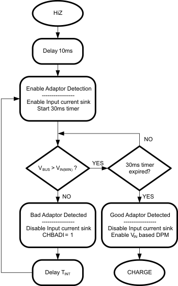 Figure 44. Bad Adaptor Detection Flow-Chart
7.4.1.3 Input Current Limiting at Start-Up
The LOW_CHG bit is automatically set when VBUS is asserted to limit the charge current to 150 mA. This ensures that a battery cannot be charged with high currents without host control.
7.4.1.4 Charge Profile
In charge mode, TPS65200 has five control loops to regulate input voltage, input current, charge current, charge voltage, and device junction temperature. During the charging process, all five loops are enabled and the one that is dominant will take over the control. The TPS65200 supports a precision Li-ion or Li-polymer charging system for single-cell applications. Figure 46 indicates a typical charge profile without input current regulation loop and it is similar to the traditional CC/CV charge curve, while Figure 47 shows a typical charge profile when input current limiting loop is dominant during the constant current mode, and in this case the charge current is higher than the input current so the charge process is faster than the linear chargers. For TPS65200, the input current limits, the charge current, termination current, and charge voltage are all programmable using I2C interface.
7.4.1.5 Precharge to Fast Charge Threshold (VSHORT)
A deeply discharged battery (VBAT < VSHORT) is charged with a constant current of ISHORT (typically 30 mA) until the voltage recovers to > VSHORT at which point fast charging begins. The pre-charge to fast-charge threshold has a default value of 2.1 V and can be adjusted by connecting a resistor from the VSHRT pin to ground. An internal current source forces a 10-µA current into the resistor and the resulting voltage is compared to half the battery voltage to determine if the battery is deeply discharged or shorted. Therefore the voltage on the VSHRT pin equals half of VSHORT threshold. For example a 100-kΩ resistor connected from VSHRT to GND results in a 2-V precharge to fast charge transition point. If the VSHRT pin is left floating or is shorted to the VDD pin, an internal reference voltage of 1.05 V is used resulting in a 2.1-V pre-charge to fast-charge threshold.
 Figure 45. Precharge to Fast-Charge Transition Threshold (VSHORT)
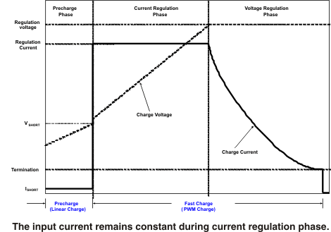 Figure 46. Typical Charging Profile of TPS65200 Without Input Current Limit
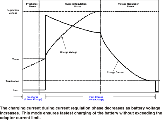 Figure 47. Typical Charging Profile of TPS65200 With Input Current Limit
7.4.1.6 PWM Controller in Charge Mode
The TPS65200 provides an integrated, fixed 3-MHz frequency voltage-mode controller with feed-forward function to regulate charge current or voltage. This type of controller is used to help improve line transient response, thereby simplifying the compensation network used for both continuous and discontinuous current conduction operation. The voltage and current loops are internally compensated using a Type-III compensation scheme that provides enough phase margin for stable operation, allowing the use of small ceramic capacitors with very low ESR. There is a 0.5-V offset on the bottom of the PWM ramp to allow the device to operate between 0% to 99.5% duty cycles.
The TPS65200 has two back-to-back common-drain N-channel MOSFETs at the high side and one N-channel MOSFET at the low side. An input N-MOSFET (Q1) prevents battery discharge when VBUS is lower than VCSOUT. The second high-side N-MOSFET (Q2) behaves as the switching control switch. A charge pump circuit is used to provide gate drive for Q1, while a boot strap circuit with external boot-strap capacitor is used to boost up the gate drive voltage for Q2.
Cycle-by-cycle current limit is sensed through the internal sense MOSFETs for Q2 and Q3. The threshold for Q2 is set to a nominal 1.9-A peak current. The low-side MOSFET (Q3) also has a current limit that decides if the PWM controller will operate in synchronous or non-synchronous mode. This threshold is set to 100mA and it turns off the low-side N-channel MOSFET (Q3) before the current reverses, preventing the battery from discharging. Synchronous operation is used when the current of the low-side MOSFET is greater than 100 mA to minimize power losses.
7.4.1.7 Battery Charging Process
During precharge phase, while the battery voltage is below the VSHORT threshold, the TPS65200 applies a short-circuit current, ISHORT, to the battery. When the battery voltage is above VSHORT and below VOREG, the charge current ramps up to fast charge current, IOCHARGE, or a charge current that corresponds to the input current of IIN_LIMIT. The slew rate for fast charge current is controlled to minimize the current and voltage over-shoot during transient. Both the input current limit (default at 100 mA), IIN_LIMIT, and fast charge current, IOCHARGE, can be set by the host. Once the battery voltage is close to the regulation voltage, VOREG, the charge current is tapered down as shown in Figure 46. The voltage regulation feedback occurs by monitoring the battery-pack voltage between the CSOUT and PGND pins. TPS65200 is a fixed single-cell voltage version, with adjustable regulation voltage (3.5 V to 4.44 V) programmed through I2C interface.
The TPS65200 monitors the charging current during the voltage regulation phase. When the termination threshold, ITERM, is detected and the battery voltage is above the recharge threshold, the TPS65200 terminates charge. The termination current level is programmable and charge termination is disabled by default. To enable the charge current termination, the host can set the charge termination bit TERM_EN of CONFIG_C register to 1. Refer to I2C section for details.
A new charge cycle is initiated when one of the following events occur:
- VBUS is power-cycled.
- CH_EN[1:0] = 11b and the battery voltage drops below the recharge threshold (TERM_EN = 1).
- The RESET bit is set (host controlled).
- The device is in CHARGE DONE state (see Figure 40) and the TERM_EN bit is set from 1 to 0.
7.4.1.8 Thermal Regulation and Protection
During the charging process, to prevent overheating of the chip, TPS65200 monitors the junction temperature, TJ, of the die and begins to taper down the charge current once TJ reaches the thermal regulation threshold, TCF. The charge current will be reduced to zero when the junction temperature increases about 10°C above TCF. At any state, if TJ exceeds TSHTDWN, TPS65200 will suspend charging and enter HiZ state. Charging will resume after TJ falls 10°C below TSHTDWN.
7.4.1.9 Safety Timer in Charge and Boost Mode (CH32MI, BST32SI)
The TPS65200 charger hosts a safety timer that stops any boost or charging action if host control is lost. The timer is started when the CH_EN[1:0] bits are set to anything different from 00 and is continuously reset by any valid I2C command. If the timer exceeds 32 s and boost mode is enabled (CH_EN[1:0] = 01b), the boost is disabled, CH_EN[1:0] is set to 00b, boost time-out fault is indicated in the INT2 register, and an interrupt is issued. Similarly, once the timer exceeds 32 minutes and the charger is enabled (CH_EN[1:0] = 10b or 11b), the charger is disabled, CH_EN[1:0] is set to 00b, charger time-out fault is indicated in INT2 register and an interrupt is issued. Time-out faults affect CH_EN[1:0] bits only and not charger parameters. The safety timer flow chart is shown in Figure 48.
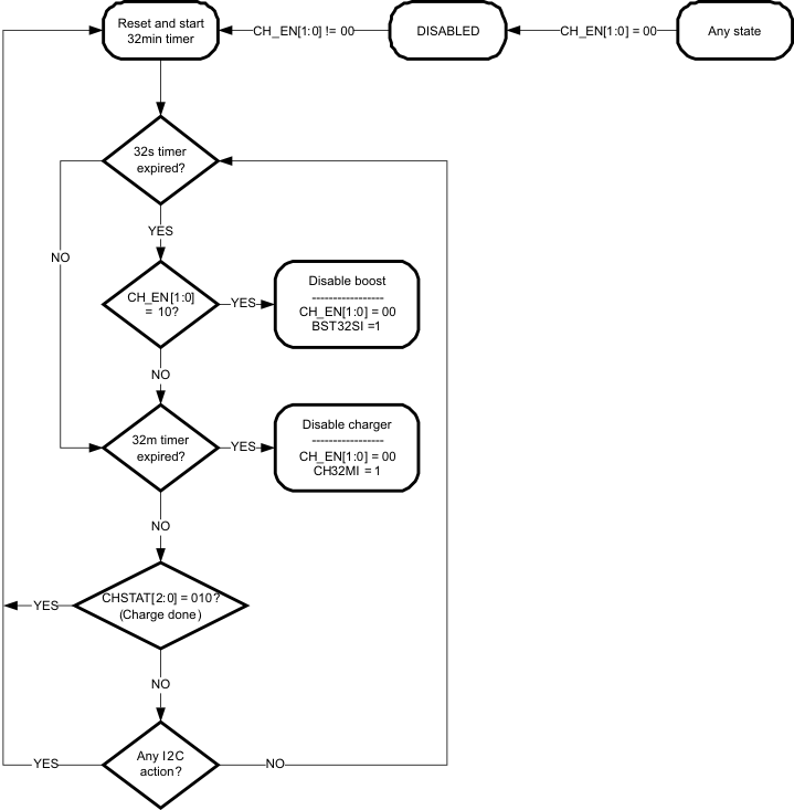 Figure 48. Timer Flow Chart for TPS65200 Charger
7.4.1.10 Input Voltage Protection in Charge Mode
7.4.1.10.1 Input Overvoltage Protection (VBUSOVPI)
The TPS65200 provides a built-in input overvoltage protection to protect the device and other components against damage if the input voltage (voltage from VBUS to PGND) gets too high. When an input overvoltage condition is detected, the TPS65200 turns off the PWM converter, sets the VBUSOVPI bit in the INT1 register and issues an interrupt. Once VVBUS drops below the input overvoltage exit threshold, the fault is cleared and charge process resumes.
7.4.1.10.2 Reverse Current Protection (CHRVPI)
The TPS65200 charger enters Hi-Z state if the voltage on VBUS pin falls below VCSOUT + VREV, and VBUS is still higher than the poor source detection threshold, VIN(MIN). The CHRVPI bit is set in the INT2 register and an interrupt is issued. This feature prevents draining the battery during the absence of VBUS. In Hi-Z mode, both the reverse blocking switch Q1 and PWM are turned off.
7.4.1.10.3 Input Voltage Based Dynamic Power Management (CHDPMI)
During normal charging process, if the input power source is not able to support the charging current, VBUS voltage will decease. Once VVBUS drops to VIN_LOW (default 4.36 V), the charge current will taper down to prevent further drop of VBUS. This feature makes the IC compatible with adaptors with different current capabilities. Whenever the VDPM loop activates, the CHDPMI interrupt is set in the INT2 register and the INT pin is pulled low. The CHDPMI interrupt is delayed by 32 ms to prevent the interrupt to occur when the charging source is removed.
7.4.1.11 Battery Protection in Charge Mode
7.4.1.11.1 Battery Charge Current Limiting
Whenever a valid power source is connected to the charger, the LOW_CHG bit of the CONFIG_C register is set to 1 which limits the charging current to 150 mA. Once the host detects that that charging source has been inserted it needs to reset the LOW_CHG bit to 0 to achieve a higher charging current. This feature prevents charging of a battery at high currents when system voltage is too low for the system to boot.
7.4.1.11.2 Output Overvoltage Protection (CHBATOVPI)
The TPS65200 provides a built-in overvoltage protection to protect the device and other components against damage if the battery voltage gets too high, as when the battery is suddenly removed. When an overvoltage condition is detected, TPS65200 turns off the PWM converter, sets the CHBATOVPI bit in the INT2 register, issues an interrupt, and enters HiZ mode. Once VCSOUT drops to the battery overvoltage exit threshold, charging resumes.
7.4.1.11.3 Battery Short Protection
During the normal charging process, if the battery voltage is lower than the short-circuit threshold, VSHORT, the charger will operate in short circuit mode with a lower charge rate of ISHORT.
7.4.1.12 Charge Status Output, STAT Pin
The STAT pin is used to indicate charging status of the IC and its behavior can be controlled by setting the STAT_EN bits of the CONTROL register. In AUTO mode, STAT is pulled low during charging and is high-impedance otherwise. STAT pin can also be forced low or to Hi-Z state by setting the STAT_EN bits accordingly. The STAT pin has enough pulldown strength to drive a LED and can be used for visual charge status indication.
7.4.2 Boost Mode Operation
In 32 second mode, when CH_EN[1:0] = 01 in CONTROL register, TPS65200 operates in boost mode and delivers power to VBUS from the battery. In normal boost mode, TPS65200 converts the battery voltage (2.5V to 4.5 V) to VBUS-B (5 V) and delivers a current as much as IBO (200 mA) to support other USB OTG devices connected to the USB connector. Boost mode can also be enabled through the OTG pin. By default the OTG pin is disabled and can be enabled by setting the OTG_EN bit to 1. The polarity of the OTG pin is user programmable through the OTG_PL bit. Both bits are located in the CONFIG_C register. The OTG pin allows the USB transceiver to take control of the boost function without involvement of the main processor.
7.4.2.1 PWM Controller in Boost Mode
Similar to charge mode operation, in boost mode, the TPS65200 provides an integrated, fixed 3-MHz frequency voltage-mode controller to regulate output voltage at PMID pin (VPMID). The voltage control loop is internally compensated using a Type-III compensation scheme that provides enough phase margin for stable operation with a wide load range and battery voltage range.
In boost mode, the input N-MOSFET (Q1) prevents battery discharge when VBUS pin is over loaded. Cycle-by-cycle current limit is sensed through the internal sense MOSFET for Q3. The threshold for Q3 is set to a nominal 1.0-A peak current. The upper-side MOSFET (Q2) also has a current limit that decides if the PWM controller will operate in synchronous or non-synchronous mode. This threshold is set to 75 mA and it turns off the high-side N-channel MOSFET (Q2) before the current reverses, preventing the battery from charging. Synchronous operation is used when the current of the high-side MOSFET is greater than 75 mA to minimize power losses.
7.4.2.2 Boost Start Up
To prevent the inductor saturation and limit the inrush current, a soft-start control is applied during the boost start up.
7.4.2.3 PFM Mode at Light Load
In boost mode, TPS65200 will operate in pulse skipping mode (PFM mode) to reduce the power loss and improve the converter efficiency at light load condition. During boosting, the PWM converter is turned off once the inductor current is less than 75 mA; and the PWM is turned back on only when the voltage at PMID pin drops to about 99.5% of the rated output voltage. A unique pre-set circuit is used to make the smooth transition between PWM and PFM mode.
7.4.2.4 Safety Timer in Boost Mode (BST32SI)
At the beginning of boost operation, the TPS65200 starts a 32-second timer that is reset by the host through any valid I2C transaction to the IC. Once the 32-second timer expires, TPS65200 will turn off the boost converter, issue an interrupt, set the BST32SI bit in the INT3 register, and return to Hi-Z mode. Fault condition is cleared by POR or reading the INT3 register.
7.4.2.5 Protection in Boost Mode
7.4.2.5.1 Output Overvoltage Protection (BSTBUSOVI)
The TPS65200 provides a built-in overvoltage protection to protect the device and other components against damage if the VBUS voltage gets too high. When an overvoltage condition is detected, TPS65200 turns off the PWM converter, resets CH_EN[1:0] bits to 00b (OFF), sets the BSTBUSOVI bit in the INT3 register, issues an interrupt, and enters HiZ mode. Once VVBUS drops to the normal level, the boost will start after host sets CH_EN[1:0] = 01b.
7.4.2.5.2 Output Over-Load Protection (BSTOLI)
The TPS65200 provides a built-in over-load protection to prevent the device and battery from damage when VBUS is over loaded. Once an over load condition is detected, Q1 will operate in linear mode to limit the output current while VPMID is kept in voltage regulation. If the over load condition lasts for more than 30 ms, the over-load fault is detected. When an over-load condition is detected, TPS65200 turns off the PWM converter, resets CH_EN[1:0] bits to 00b (OFF), sets the BSTOLI bit in the INT3 register, and issues an interrupt. The boost will not start until the host sets CH_EN[1:0] = 01b or the OTG pin is toggled.
7.4.2.5.3 Battery Voltage Protection (BSTLOWVI, BSTBATOVI)
During boosting, when battery voltage is above the battery overvoltage threshold, VBATMAX, or below the minimum battery voltage threshold, VBATMIN, TPS65200 will turn off the PWM converter, reset CH_EN[1:0] bits to 00b (OFF), set the BSTLOWVI or BSTBATOVI bit in the INT3 register, and issues an interrupt. Once the battery voltage goes back to the normal level, the boost will start if the host sets CH_EN[1:0] = 01b or the OTG pin is toggled.
7.4.3 High Impedance Mode
When CH_EN[1:0] bits in the CONTROL register are set to 00b, TPS65200 will operate in high impedance mode, with the impedance looking into VBUS pin higher than 500kΩ.
7.5 Programming
7.5.1 I2C Bus Operation
The TPS65200 hosts a slave I2C interface that supports data rates up to 400 kbit/s and auto-increment addressing and is compliant to I2C standard 3.0.
 Figure 49. Subaddress in I2C Transmission
| Start – Start Condition | ACK – Acknowledge |
| G(3:0) – Group ID: Address fixed at 1101 | S(7:0) – Subaddress: defined per register map |
| A(2:0) – Device Address: Address fixed at 010 | D(7:0) – Data; Data to be loaded into the device |
| R/nW – Read / not Write Select Bit | Stop – Stop Condition |
The I2C bus is a communications link between a controller and a series of slave terminals. The link is established using a two-wired bus consisting of a serial clock signal (SCL) and a serial data signal (SDA). The serial clock is sourced from the controller in all cases where the serial data line is bi-directional for data communication between the controller and the slave terminals. Each device has an open drain output to transmit data on the serial data line. An external pull-up resistor must be placed on the serial data line to pull the drain output high during data transmission.
Data transmission is initiated with a start bit from the controller as shown in Figure 50. The start condition is recognized when the SDA line transitions from high to low during the high portion of the SCL signal. Upon reception of a start bit, the device will receive serial data on the SDA input and check for valid address and control information. If the appropriate group and address bits are set for the device, then the device will issue an acknowledge pulse and prepare the receive subaddress data. Subaddress data is decoded and responded to as per the Register Map section of this document. Data transmission is completed by either the reception of a stop condition or the reception of the data word sent to the device. A stop condition is recognized as a low to high transition of the SDA input during the high portion of the SCL signal. All other transitions of the SDA line must occur during the low portion of the SCL signal. An acknowledge is issued after the reception of valid address, sub-address and data words. The I2C interface will auto-sequence through register addresses, so that multiple data words can be sent for a given I2C transmission.
 Figure 50. I2C Start/Stop/Acknowledge Protocol
7.6 Register Maps
Table 1. Register Address Map
| REGISTER | ADDRESS (HEX) |
NAME | DEFAULT VALUE |
DESCRIPTION |
|---|---|---|---|---|
| 0 | 0 | CONTROL | 0000 1010 | Enable control register |
| 1 | 1 | CONFIG_A | 0000 0001 | Charger current register |
| 2 | 2 | CONFIG_B | 0001 1001 | Charger voltage register |
| 3 | 3 | CONFIG_C | 1000 1010 | Special charger settings |
| 4 | 4 | CONFIG_D | 0100 0000 | Charger safety limits settings |
| 5 | 5 | WLED | 0001 1111 | WLED feedback voltage setting |
| 6 | 6 | STATUS_A | 0100 0000 | Status register A |
| 7 | 7 | STATUS_B | 0000 0001 | Status register B |
| 8 | 8 | INT1 | 0000 0000 | Interrupt bits |
| 9 | 9 | INT2 | 0000 0000 | Interrupt bits (charger) |
| 10 | 0A | INT3 | 0000 0000 | Interrupt bits (boost) |
| 11 | 0B | MASK1 | 0000 0000 | Interrupt masking bits |
| 12 | 0C | MASK2 | 0000 0000 | Interrupt masking bits |
| 13 | 0D | MASK3 | 0000 0000 | Interrupt masking bits |
| 14 | 0E | CHIPID | 0000 0000 | Chip ID register |
7.6.1 Control Register (CONTROL)
Address – 0x00h| DATA BIT | D7 | D6 | D5 | D4 | D3 | D2 | D1 | D0 |
|---|---|---|---|---|---|---|---|---|
| FIELD NAME | STAT_EN[1:0] | SMON_EN | WLED_EN | LDO_EN | DPDM_EN | CH_EN [1:0] | ||
| READ/WRITE | R/W | R/W | R/W | R/W | R/W | R/W | R/W | R/W |
| RESET VALUE | 0 | 0 | 0 | 0 | 1 | 0 | 1 | 0 |
| FIELD NAME | BIT DEFINITION |
|---|---|
| STAT_EN[1:0 | STAT enable bits |
| 00 – AUTO (controlled by charger status) | |
| 01 – ON (low impedance) | |
| 10 – OFF (high impedance) | |
| 11 – not defined | |
| SMON_EN | Shunt monitor enable bit |
| 0 – Disabled | |
| 1 – Enabled | |
| WLED_EN | WLED enable bit |
| 0 – Disabled | |
| 1 – Enabled | |
| NOTE: WLED can also be enabled through CTRL pin. | |
| LDO_EN | LDO enable bit |
| 0 – Disabled | |
| 1 – Enabled | |
| DPDM_EN | D+/D- detection enable |
| 0 – Disabled | |
| 1 – Enabled | |
| NOTE: Bit is automatically reset after detection is completed. | |
| CH_EN[1:0] | Charger enable bits |
| 00 – Disabled / HiZ mode | |
| 01 – Boost mode | |
| 10 – Charge | |
| 11 – Charge with automatic recharge |
7.6.2 Charger Config Register A (CONFIG_A)
Address – 0x01h| DATA BIT | D7 | D6 | D5 | D4 | D3 | D2 | D1 | D0 |
|---|---|---|---|---|---|---|---|---|
| FIELD NAME | LMTSEL | VICHRG[3:0] | VITERM[2:0] | |||||
| READ/WRITE | R/W | R/W | R/W | R/W | R/W | R/W | R/W | R/W |
| RESET VALUE | 0 | 0 | 0 | 0 | 0 | 0 | 0 | 1 |
| FIELD NAME | BIT DEFINITION(1) |
|---|---|
| LMTSEL | Input Current Limit selction |
| 0 – Input current limit is set to the higher of IIN_LIMIT[1:0] (CONFIG_B) and D+D- det. result | |
| 1 – IIN_LIMIT[1:0] (CONFIG_B) applied, D+D- detection result is ignored | |
| VICHRG[3:0] | Charge current sense voltage (current equivalent for 20 mΩ shunt) |
| 0000 – 11 mV (550 mA) | |
| 0001 – 13 mV (650 mA) | |
| 0010 – 15 mV (75 mA) | |
| 0011 – 17 mV (850 mA) | |
| 0100 – 19 mV (950 mA) | |
| 0101 – 21 mV (105 mA) | |
| 0101 – 21 mV (1050 mA) | |
| 0110 – 23 mV (1150 mA) | |
| 0111 – 25 mV (1250 mA) | |
| 1000 – 27 mV (1350 mA) | |
| 1001 – 29 mV (1450 mA) | |
| 1010 – 31 mV (1550 mA) | |
| ... | |
| 1111 – 31 mV (1550 mA) | |
| VITERM[2:0] | Termination current sense voltage (current equivalent for 20 mΩ shunt) |
| 000 – 1 mV (50 mA) | |
| 001 – 2 mV (100 mA) | |
| 010 – 3 mV (150 mA) | |
| 011 – 4 mV (200 mA) | |
| 100 – 5 mV (250 mA) | |
| 101 – 6 mV (300 mA) | |
| 110 – 7 mV (350 mA) | |
| 111 – 8 mV (400 mA) |
7.6.3 Charger Config Register B (CONFIG_B)
Address – 0x02h| DATA BIT | D7 | D6 | D5 | D4 | D3 | D2 | D1 | D0 |
|---|---|---|---|---|---|---|---|---|
| FIELD NAME | IIN_LIMIT[1:0] | VOREG[5:0] | ||||||
| READ/WRITE | R/W | R/W | R/W | R/W | R/W | R/W | R/W | R/W |
| RESET VALUE | 0 | 0 | 0 | 1 | 1 | 0 | 0 | 1 |
| FIELD NAME | BIT DEFINITION(1) |
|---|---|
| IIN_LIMIT[1:0] | Input current limit setting |
| 00 – 100 mA | |
| 01 – 500 mA | |
| 10 – 975 mA | |
| 11 – No input current limit | |
| VOREG[5:0] | Battery regulation voltage / boost output voltage |
| 00 0000 – 3.50 V / 4.425 V | |
| 00 0001 – 3.52 V / 4.448 V | |
| 00 0011 – 3.56 V / 4.471 V | |
| ... | |
| 01 1000 – 3.98 V / 4.077 V | |
| 01 1001 – 4.00 V / 5 V | |
| 01 1010 – 4.02 V / 5.023 V | |
| ... | |
| 10 1111 – 4.44 V / 5.5 V | |
| ... | |
| 11 1111 – 4.44 V / 5.5 V |
7.6.4 Charger Config Register C (CONFIG_C)
Address – 0x03h| DATA BIT | D7 | D6 | D5 | D4 | D3 | D2 | D1 | D0 |
|---|---|---|---|---|---|---|---|---|
| FIELD NAME | VS_REF | OTG_PL | OTG_EN | TERM_EN | LOW_CHG | VSREG[2:0] | ||
| READ/WRITE | R/W | R/W | R/W | R/W | R/W | R/W | R/W | R/W |
| RESET VALUE | 1 | 0 | 0 | 0 | 1 | 0 | 1 | 0 |
| FIELD NAME | BIT DEFINITION |
|---|---|
| VS_REF | VSHORT reference select |
| 0 – Internal (2.1 V) reference | |
| 1 – Current source on VSHRT pin is enabled. Pin voltage is used as 0.5 x VSHORT threshold. | |
| OTG_PL | OTG pin polarity |
| 0 – Active low | |
| 1 – Active high | |
| OTG_EN | OTG pin enable |
| 0 – Pin is disabled | |
| 1 – Pin is enabled | |
| TERM_EN | Charge termination enable |
| 0 – Disabled | |
| 1 – Enabled | |
| LOW_CHG | Low charge current enable bit (current equivalent for 20 mΩ shunt) |
| 0 – Normal charge current sense voltage per register CONFIG_A | |
| 1 – 3 mV (150 mA) | |
| VSREG[2:0] | Input voltage DPM regulation voltage |
| 000 – 4.20 V | |
| 001 – 4.28 V | |
| 010 – 4.36 V | |
| 011 – 4.44 V | |
| 100 – 4.52 V | |
| 101 – 4.60 V | |
| 110 – 4.68 V | |
| 111 – 4.76 V |
7.6.5 Charger Config Register D (CONFIG_D)
Address – 0x04h| DATA BIT | D7 | D6 | D5 | D4 | D3 | D2 | D1 | D0 |
|---|---|---|---|---|---|---|---|---|
| FIELD NAME | VMCHRG[3:0] | VMREG[3:0] | ||||||
| READ/WRITE | R/W | R/W | R/W | R/W | R/W | R/W | R/W | R/W |
| RESET VALUE | 0 | 1 | 0 | 0 | 0 | 0 | 0 | 0 |
| FIELD NAME | BIT DEFINITION(1) |
|---|---|
| VMCHRG[3:0] | Maximum charge current sense voltage (current equivalent for 20 mΩ shunt) |
| 0000 – 11 mV (550 mA) | |
| 0001 – 13 mV (650 mA) | |
| 0010 – 15 mV (750 mA) | |
| 0011 – 17 mV (850 mA) | |
| 0100 – 19 mV (950 mA) | |
| 0101 – 21 mV (1050 mA) | |
| 0110 – 23 mV (1150 mA) | |
| 0111 – 25 mV (1250 mA) | |
| 1000 – 27 mV (1350 mA) | |
| 1001 – 29 mV (1450 mA) | |
| 1010 – 31 mV (1550 mA) | |
| … | |
| 1111 – 31 mV (1550 mA) | |
| VMREG[3:0] | Maximum battery regulation voltage |
| 0000 – 4.20 V | |
| 0001 – 4.22 V | |
| 0010 – 4.24 V | |
| … | |
| 1100 – 4.44 V | |
| ... | |
| 1111 – 4.44 V |
7.6.6 WLED Control Register (WLED)
Address – 0x05h| DATA BIT | D7 | D6 | D5 | D4 | D3 | D2 | D1 | D0 |
|---|---|---|---|---|---|---|---|---|
| FIELD NAME | Not used | Not used | Not used | VFB[4:0] | ||||
| READ/WRITE | R | R | R | R/W | R/W | R/W | R/W | R/W |
| RESET VALUE | 0 | 0 | 0 | 1 | 1 | 1 | 1 | 1 |
| FIELD NAME | BIT DEFINITION |
|---|---|
| Not used | N/A |
| Not used | N/A |
| Not used | N/A |
| VFB[4:0 | WLED feedback voltage |
| 0 0000 – 0% | |
| 0 0001 – 2.5% | |
| 0 0010 – 4% | |
| 0 0011 – 5.5% | |
| 0 0100 – 7.5% | |
| 0 0101 – 8.5% | |
| 0 0110 – 10% | |
| 0 0111 – 11.5% | |
| 0 1000 – 13% | |
| 0 1001 – 14.5% | |
| 0 1010 – 16% | |
| 0 1011 – 17.5% | |
| 0 1100 – 19% | |
| 0 1101 – 22% | |
| 0 1110 – 25% | |
| 0 1111 – 28% | |
| 1 0000 – 31% | |
| 1 0001 – 34% | |
| 1 0010 – 37% | |
| 1 0011 – 40% | |
| 1 0100 – 43% | |
| 1 0101 – 46% | |
| 1 0110 – 49% | |
| 1 0111 – 52% | |
| 1 1000 – 58% | |
| 1 1001 – 64% | |
| 1 1010 – 70% | |
| 1 1011 – 76% | |
| 1 1100 – 82% | |
| 1 1101 – 88% | |
| 1 1110 – 94% | |
| 1 1111 – 100% |
7.6.7 Status Register A (STATUS_A)
Address – 0x06h| DATA BIT | D7 | D6 | D5 | D4 | D3 | D2 | D1 | D0 |
|---|---|---|---|---|---|---|---|---|
| FIELD NAME | Not used | STANDBY | MONITOR | CHSTAT [2:0] | LDO | WLED | ||
| READ/WRITE | R | R | R | R | R | R | R | R |
| RESET VALUE | 0 | 1 | 0 | 0 | 0 | 0 | 0 | 0 |
| FIELD NAME | BIT DEFINITION(1) |
|---|---|
| Not used | N/A |
| STANDBY | Standby status indicator |
| 0 – Device is in ACTIVE mode | |
| 1 – Device is in STANDBY mode | |
| MONITOR | Current shunt monitor status indicator |
| 0 – Current shunt monitor is disabled | |
| 1 – Current shunt monitor is enabled | |
| CHSTAT [2:0] | Charger status bit |
| 000 – High impedance mode | |
| 001 – Charge in progress (fast charge) | |
| 010 – Charge done | |
| 011 – Boost mode | |
| 100 – Charge in progress (pre charge) | |
| 101 – Not defined | |
| 110 – Not defined | |
| 111 – Not defined | |
| LDO | LDO status bit |
| 0 – LDO is disabled (OFF) | |
| 1 – LDO is enabled (ON), no fault | |
| WLED | WLED status bit |
| 0 – WLED disabled (OFF) | |
| 1 – WLED enabled |
7.6.8 Status Register B (STATUS_B)
Address – 0x07h| DATA BIT | D7 | D6 | D5 | D4 | D3 | D2 | D1 | D0 |
|---|---|---|---|---|---|---|---|---|
| FIELD NAME | RESET | Not used | Not used | Not used | Not used | DPDM_D | DPDM_R | OTG |
| READ/WRITE | W | R | R | R | R | R | R | R |
| RESET VALUE | 0 | 0 | 0 | 0 | 0 | 0 | 0 | 1 |
| FIELD NAME | BIT DEFINITION(1) |
|---|---|
| RESET | Reset |
| 0 – No effect | |
| 1 – Reset all parameters to default values | |
| NOTE: Read always returns “0” | |
| Not used | N/A |
| Not used | N/A |
| Not used | N/A |
| Not used | N/A |
| DPDM_D | D+/D- detection done bit |
| 0 – DPDM detection in progress or not started after initial power-up reset | |
| 1 – DPDM detection is complete | |
| DPDM_R | D+D- detection result |
| 0 – Standard USB port (500-mA current limit) | |
| 1 – USB charger (1000-mA current limit) | |
| OTG | OTG pin status |
| 0 – OTG pin at low level | |
| 1 – OTG pin at high level |
7.6.9 Interrupt Register 1 (INT1)
Address – 0x08h| DATA BIT | D7 | D6 | D5 | D4 | D3 | D2 | D1 | D0 |
|---|---|---|---|---|---|---|---|---|
| FIELD NAME | TSDI | VBUSOVPI | Not used | Not used/ Reserved |
Not used/ Reserved |
Not used/ Reserved |
Not used/ Reserved |
WLEDI |
| READ/WRITE | R | R | R | R/W | R/W | R/W | R/W | R |
| RESET VALUE | 0 | 0 | 0 | 0 | 0 | 0 | 0 | 0 |
| FIELD NAME | BIT DEFINITION |
|---|---|
| TSDI | Thermal shutdown fault. Set if die temperature exceeds thermal shutdown threshold. Reset when die temperature drops below TSD release threshold. |
| VBUSOVPI | VBUS overvoltage protection. Set when VBUS > VOVP-IN_USB is detected. |
| Not used | N/A |
| Not used / Reserved | N/A / Reserved |
| Not used / Reserved | N/A / Reserved |
| Not used / Reserved | N/A / Reserved |
| Not used / Reserved | N/A / Reserved |
| WLEDI | WLED driver over voltage |
7.6.10 Interrupt Register 2 (INT2)
Address – 0x09h| DATA BIT | D7 | D6 | D5 | D4 | D3 | D2 | D1 | D0 |
|---|---|---|---|---|---|---|---|---|
| FIELD NAME | CHRVPI | CHBADI | CHBATOVI | CHTERMI | CHRCHGI | CH32MI | CHTREGI | CHDPMI |
| READ/WRITE | R | R | R | R | R | R | R | R |
| RESET VALUE | 0 | 0 | 0 | 0 | 0 | 0 | 0 | 0 |
| FIELD NAME | BIT DEFINITION(1) |
|---|---|
| CHRVPI | Charger fault. Reverse protection (VVBUS > VIN(MIN) and VVBUS < VCSOUT+VREV (fault) |
| CHBADI | Charger fault. Bad adaptor (VBUS < VIN(MIN)) |
| CHBATOVI | Charger fault. Battery OVP |
| CHTERMI | Charge terminated |
| CHRCHGI | Recharge request (VCSOUT < VOREG – VRCH) |
| CH32MI | Charger fault. 32 m time-out (fault) |
| CHTREGI | Charger warning. Thermal regulation loop active. |
| CHDPMI | Charger warning. Input voltage DPM loop active. |
7.6.11 Interrupt Register 3 (INT3)
Address – 0x0Ah| DATA BIT | D7 | D6 | D5 | D4 | D3 | D2 | D1 | D0 |
|---|---|---|---|---|---|---|---|---|
| FIELD NAME | BSTBUSOVI | BSTOLI | BSTLOWVI | BSTBATOVI | BST32SI | Not used | Not used | Not used |
| READ/WRITE | R | R | R | R | R | R | R | R |
| RESET VALUE | 0 | 0 | 0 | 0 | 0 | 0 | 0 | 0 |
| FIELD NAME | BIT DEFINITION(1) |
|---|---|
| BSTBUSOVI | Boost fault. VBUS OVP (VBUS > VBUSOVP) |
| BSTOLI | Boost fault. Over load. |
| BSTLOWVI | Boost fault. Battery voltage is too low. |
| BSTBATOVI | Boost fault. Battery over voltage. |
| BST32SI | Boost fault. 32-s time-out fault. |
| Not used | N/A |
| Not used | N/A |
| Not used | N/A |
7.6.12 Interrupt Mask Register 1 (MASK1)
Address – 0x0Bh| DATA BIT | D7 | D6 | D5 | D4 | D3 | D2 | D1 | D0 |
|---|---|---|---|---|---|---|---|---|
| FIELD NAME | TSDM | VBUSOVPM | Not used | Not used | Not used | Not used | Not used | WLEDM |
| READ/WRITE | R/W | R/W | R/W | R/W | R/W | R/W | R/W | R/W |
| RESET VALUE | 0 | 0 | 0 | 0 | 0 | 0 | 0 | 0 |
| FIELD NAME | BIT DEFINITION(1) |
|---|---|
| TSDM | TSD fault interrupt mask |
| 0 – Interrupt not masked | |
| 1 – Interrupt masked | |
| VBUSOVPM | VBUS OVP fault interrupt mask |
| 0 – Interrupt not masked | |
| 1 – Interrupt masked | |
| Not used | N/A |
| Not used | N/A |
| Not used | N/A |
| Not used | N/A |
| Not used | N/A |
| WLEDM | WLED fault interrupt mask |
| 0 – Interrupt not masked | |
| 1 – Interrupt masked |
7.6.13 Interrupt Mask Register 2 (MASK2)
Address – 0x0Ch| DATA BIT | D7 | D6 | D5 | D4 | D3 | D2 | D1 | D0 |
|---|---|---|---|---|---|---|---|---|
| FIELD NAME | CHRVPM | CHBADM | CHBATOVM | CHTERMM | CHRCHGM | CH32MM | CHTREGM | CHDPMM |
| READ/WRITE | R/W | R/W | R/W | R/W | R/W | R/W | R/W | R/W |
| RESET VALUE | 0 | 0 | 0 | 0 | 0 | 0 | 0 | 0 |
| FIELD NAME | BIT DEFINITION(1) |
|---|---|
| CHRVPM | Charger reverse protection interrupt mask |
| 0 – Interrupt not masked | |
| 1 – Interrupt masked | |
| CHBADM | Charger Bad adaptor interrupt mask |
| 0 – Interrupt not masked | |
| 1 – Interrupt masked | |
| CHBATOVM | Charger battery overvoltage interrupt mask |
| 0 – Interrupt not masked | |
| 1 – Interrupt masked | |
| CHTERMM | Charge terminated interrupt mask |
| 0 – Interrupt not masked | |
| 1 – Interrupt masked | |
| CHRCHGM | Charger recharge request interrupt mask |
| 0 – Interrupt not masked | |
| 1 – Interrupt masked | |
| CH32MM | Charger 32m timeout interrupt mask |
| 0 – Interrupt not masked | |
| 1 – Interrupt masked | |
| CHTREGM | Charger thermal regulation loop active interrupt mask |
| 0 – Interrupt not masked | |
| 1 – Interrupt masked | |
| CHDPMM | Charger input current DPM active interrupt mask |
| 0 – Interrupt not masked | |
| 1 – Interrupt masked |
7.6.14 Interrupt Mask Register 3 (MASK3)
Address – 0x0Dh| DATA BIT | D7 | D6 | D5 | D4 | D3 | D2 | D1 | D0 |
|---|---|---|---|---|---|---|---|---|
| FIELD NAME | BSTBUSOVM | BSTOLM | BSTLOWVM | BSTBATOVM | BST32SM | Not used | Not used | Not used |
| READ/WRITE | R/W | R/W | R/W | R/W | R/W | R/W | R/W | R/W |
| RESET VALUE | 0 | 0 | 0 | 0 | 0 | 0 | 0 | 0 |
| FIELD NAME | BIT DEFINITION(1) |
|---|---|
| BSTBUSOVM | Boost VBUS overvoltage interrupt mask |
| 0 – Interrupt not masked | |
| 1 – Interrupt masked | |
| BSTOLM | Boost over load interrupt mask |
| 0 – Interrupt not masked | |
| 1 – Interrupt masked | |
| BSTLOWVM | Boost low battery voltage interrupt mask |
| 0 – Interrupt not masked | |
| 1 – Interrupt masked | |
| BSTBATOVM | Boost battery overvoltage interrupt mask |
| 0 – Interrupt not masked | |
| 1 – Interrupt masked | |
| BST32SM | Boost 32s time out interrupt mask |
| 0 – Interrupt not masked | |
| 1 – Interrupt masked | |
| Not used | N/A |
| Not used | N/A |
| Not used | N/A |
7.6.15 Chip ID Register (CHIPID)
Address – 0x0Eh| DATA BIT | D7 | D6 | D5 | D4 | D3 | D2 | D1 | D0 |
|---|---|---|---|---|---|---|---|---|
| FIELD NAME | VENDOR[1:0] | CHIP[2:0] | REV[2:0] | |||||
| READ/WRITE | R | R | R | R | R | R | R | R |
| RESET VALUE | 0 | 0 | 0 | 0 | 0 | 0 | 0 | 1(1) |
| FIELD NAME | BIT DEFINITION |
|---|---|
| VENDOR[1:0] | Vendor code 00 – default |
| 00 – Default | |
| CHIP[2:0] | Chip ID |
| 000 – TPS65200 | |
| 001 – Future use | |
| ... | |
| 111 – Future use | |
| REV[2:0] | Revision code |
| 000 – Revision 1.0 | |
| 001 – Revision 1.1 | |
| 010 – Future use | |
| ... | |
| 111 – Future use |