SLVSB64I November 2011 – March 2018 TPS65217
PRODUCTION DATA.
- 1 Features
- 2 Applications
- 3 Description
- 4 Revision History
- 5 Device Comparison Table
- 6 Pin Configuration and Functions
- 7 Specifications
-
8 Detailed Description
- 8.1 Overview
- 8.2 Functional Block Diagram
- 8.3
Feature Description
- 8.3.1 Wake-Up and Power-Up Sequencing
- 8.3.2 Power Good
- 8.3.3 Push-Button Monitor (PB_IN)
- 8.3.4 nWAKEUP Pin (nWAKEUP)
- 8.3.5 Power Enable Pin (PWR_EN)
- 8.3.6 Reset Pin (nRESET)
- 8.3.7 Interrupt Pin (nINT)
- 8.3.8 Analog Multiplexer
- 8.3.9 Battery Charger and Power Path
- 8.3.10 Battery Charging
- 8.3.11 Precharge
- 8.3.12 Charge Termination
- 8.3.13 Battery Detection and Recharge
- 8.3.14 Safety Timer
- 8.3.15 Battery-Pack Temperature Monitoring
- 8.3.16 DC/DC Converters
- 8.3.17 Standby LDO Regulators (LDO1, LDO2)
- 8.3.18 Load Switches or LDO Regulators (LS1 or LDO3, LS2 or LDO4)
- 8.3.19 White LED Driver
- 8.4 Device Functional Modes
- 8.5 Programming
- 8.6
Register Maps
- 8.6.1 Register Address Map
- 8.6.2 Chip ID Register (CHIPID) (Address = 0x00) [reset = X]
- 8.6.3 Power Path Control Register (PPATH) (Address = 0x01) [reset = 0x3D]
- 8.6.4 Interrupt Register (INT) (Address = 0x02) [reset = 0x80]
- 8.6.5 Charger Configuration Register 0 (CHGCONFIG0) (Address = 0x03) [reset = 0x00]
- 8.6.6 Charger Configuration Register 1 (CHGCONFIG1) (Address = 0x04) [reset = 0xB1]
- 8.6.7 Charger Configuration Register 2 (CHGCONFIG2) (Address = 0x05) [reset = 0x80]
- 8.6.8 Charger Configuration Register 3 (CHGCONFIG3) (Address = 0x06) [reset = 0xB2]
- 8.6.9 WLED Control Register 1 (WLEDCTRL1) (Address = 0x07) [reset = 0xB1]
- 8.6.10 WLED Control Register 2 (WLEDCTRL2) (Address = 0x08) [reset = 0x00]
- 8.6.11 MUX Control Register (MUXCTRL) (Address = 0x09) [reset = 0x00]
- 8.6.12 Status Register (STATUS) (Address = 0x0A) [reset = 0x00]
- 8.6.13 Password Register (PASSWORD) (Address = 0x0B) [reset = 0x00]
- 8.6.14 Power Good Register (PGOOD) (Address = 0x0C) [reset = 0x00]
- 8.6.15 Power-Good Control Register (DEFPG) (Address = 0x0D) [reset = 0x0C]
- 8.6.16 DCDC1 Control Register (DEFDCDC1) (Address = 0x0E) [reset = X]
- 8.6.17 DCDC2 Control Register (DEFDCDC2) (Address = 0x0F) [reset = X]
- 8.6.18 DCDC3 Control Register (DEFDCDC3) (Address = 0x10) [reset = 0x08]
- 8.6.19 Slew-Rate Control Register (DEFSLEW) (Address = 0x11) [reset = 0x06]
- 8.6.20 LDO1 Control Register (DEFLDO1) (Address = 0x12) [reset = 0x09]
- 8.6.21 LDO2 Control Register (DEFLDO2) (Address = 0x13) [reset = 0x38]
- 8.6.22 Load Switch1 or LDO3 Control Register (DEFLS1) (Address = 0x14) [reset = X]
- 8.6.23 Load Switch2 or LDO4 Control Register (DEFLS2) (Address = 0x15) [reset = X]
- 8.6.24 Enable Register (ENABLE) (Address = 0x16) [reset = 0x00]
- 8.6.25 UVLO Control Register (DEFUVLO) (Address = 0x18) [reset = 0x03]
- 8.6.26 Sequencer Register 1 (SEQ1) (Address = 0x19) [reset = X]
- 8.6.27 Sequencer Register 2 (SEQ2) (Address = 0x1A) [reset = X]
- 8.6.28 Sequencer Register 3 (SEQ3) (Address = 0x1B) [reset = X]
- 8.6.29 Sequencer Register 4 (SEQ4) (Address = 0x1C) [reset = 0x40]
- 8.6.30 Sequencer Register 5 (SEQ5) (Address = 0x1D) [reset = X]
- 8.6.31 Sequencer Register 6 (SEQ6) (Address = 0x1E) [reset = 0x00]
- 9 Application and Implementation
- 10Power Supply Recommendations
- 11Layout
- 12Device and Documentation Support
- 13Mechanical, Packaging, and Orderable Information
Package Options
Mechanical Data (Package|Pins)
- RSL|48
Thermal pad, mechanical data (Package|Pins)
- RSL|48
Orderable Information
8.3.9 Battery Charger and Power Path
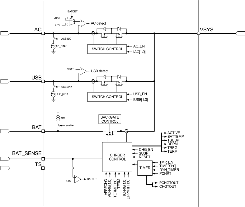
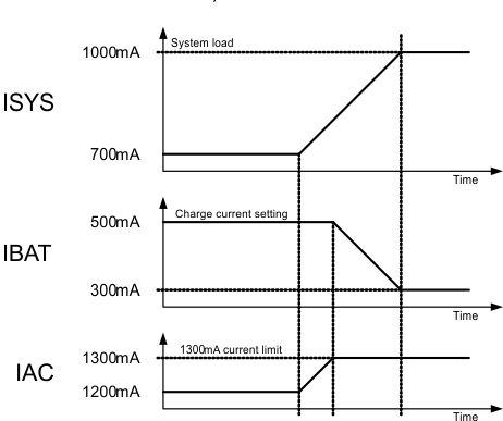
The TPS65217x device has a linear charger for Li+ batteries and a triple system-power path targeted at space-limited portable applications. The power path lets simultaneous and independent charging of the battery and powering of the system. This feature enables the system to run with a defective or absent battery pack and lets instant system turnon even with a totally discharged battery. The input power source for charging the battery and running the system can be either an AC adapter or a USB port. The power path prioritizes the AC input over the USB input, and both over the battery input, to decrease the number of charge and discharge cycles on the battery. Charging current is automatically decreased when the system load increases to the point where the AC or USB power supply reach the maximum allowable current. If the AC or USB power supply cannot provide enough current to the system, the battery supplies the additional current required and the battery will discharge until the system load is reduced. Figure 11 shows a block diagram of the power path. Figure 12 shows an example of the power path management function.
 Figure 11. Block Diagram of the Power Path and Battery Charger

The detection thresholds for AC and USB inputs are a function of the battery voltage, and three basic use cases must be considered: shorted or absent battery, dead battery, and good battery.