-
TPS65235-1 LNB Voltage Regulator With I2C Interface
- 1 Features
- 2 Applications
- 3 Description
- 4 Revision History
- 5 Pin Configuration and Functions
- 6 Specifications
-
7 Detailed Description
- 7.1 Overview
- 7.2 Functional Block Diagram
- 7.3
Feature Description
- 7.3.1 Boost Converter
- 7.3.2 Linear Regulator and Current Limit
- 7.3.3 Boost Converter Current Limit
- 7.3.4 Charge Pump
- 7.3.5 Slew Rate Control
- 7.3.6 Short-Circuit Protection, Hiccup, and Overtemperature Protection
- 7.3.7 Tone Generation
- 7.3.8 Tone Detection
- 7.3.9 Audio Noise Rejection
- 7.3.10 Disable and Enable
- 7.3.11 Component Selection
- 7.4 Device Functional Modes
- 7.5 Programming
- 7.6 Register Maps
- 8 Application and Implementation
- 9 Device and Documentation Support
- 10Mechanical, Packaging, and Orderable Information
- IMPORTANT NOTICE
Package Options
Mechanical Data (Package|Pins)
- RUK|20
Thermal pad, mechanical data (Package|Pins)
- RUK|20
Orderable Information
TPS65235-1 LNB Voltage Regulator With I2C Interface
1 Features
- Complete integrated solution for LNB and I2C interface
- DiSEqC 2.x, and DiSEqC 1.x compatible
- Supports 5-V, 12-V, and 15-V power rail
- Up to 1000-mA accurate output current limit adjustable by external resistor
- Boost switch peak current limit proportional to LDO current limit
- Boost converter with 140-mΩ low Rds(on) internal power switch
- Boost switching frequency 1-MHz or 500-kHz selectable
- Audible noise avoided at force PWM mode
- Dedicated enable pin for non-I2C application
- Low-dropout (LDO) regulator with push-pull output stage for VLNB output
- Built-in accurate 22-kHz tone generator and external tone input support
- Supports both external 44-kHz and 22-kHz tone input
- Adjustable soft start and 13-V to 18-V voltage transition time
- 650-mV to 750-mV 22-kHz tone amplitude selection
- I2C registers accessible with EN low
- Short circuit dynamic protection
- Diagnostics for output voltage level, DiSEqC tone input and output, current level, and cable connection
- Thermal protection available
- 20-pin WQFN 3-mm × 3-mm (RUK) package
3 Description
Designed for analog and digital satellite receivers, the TPS65235-1 is a monolithic voltage regulator with I2C interface; specifically to provide the 13-V to 18-V power supply and the 22-kHz tone signal to the LNB down converter in the antenna dish or to the multi-switch box. The device offers a complete solution with minimum component count, low power dissipation together with simple design and I2C standard interface.
The TPS65235-1 features high power efficiency. The boost converter integrates a 140-mΩ power MOSFET running at 1-MHz or 500-kHz selectable switching frequency. Drop out voltage at the linear regulator is 0.8 V to minimize power loss. The TPS65235-1 provides multiple ways to generate the 22-kHz signal. Integrated linear regulator with push-pull output stage generates 22-kHz tone signal superimposed at the output even at zero loading. Current limit of linear regulator can be programmed by external resistor with ±10% accuracy. Full range of diagnostic read by I2C is available for system monitoring.
The TPS65235-1 has a special design at FCCM mode to avoid the audible noise especially when VIN is higher or closer to the VLNB output.
The TPS65235-1 supports advanced DiSEqC 2.x standard with 22-kHz tone detection circuit and output interface.
| PART NUMBER | PACKAGE | BODY SIZE (NOM) |
|---|---|---|
| TPS65235-1 | RUK (WQFN, 20) | 3.00 mm × 3.00 mm |
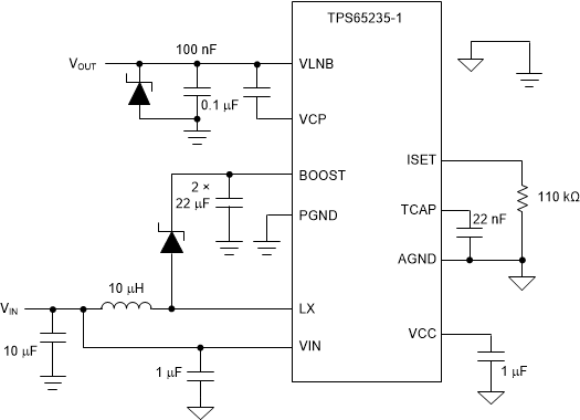
 Simplified Schematic