SLVSCF9D january   2014  – may 2023 TPS65262

PRODUCTION DATA  

  1.   1
  2. Features
  3. Applications
  4. Description
  5. Revision History
  6. Pin Configuration and Functions
  7. Specifications
    1. 6.1 Absolute Maximum Ratings
    2. 6.2 ESD Ratings
    3. 6.3 Recommended Operating Conditions
    4. 6.4 Thermal Information
    5. 6.5 Electrical Characteristics
    6. 6.6 Typical Characteristics
  8. Detailed Description
    1. 7.1 Overview
    2. 7.2 Functional Block Diagram
    3. 7.3 Feature Description
      1. 7.3.1  Adjusting the Output Voltage
      2. 7.3.2  Enable and Adjusting Undervoltage Lockout
      3. 7.3.3  Soft-Start Time
      4. 7.3.4  Power-Up Sequencing
        1. 7.3.4.1 External Power Sequencing
        2. 7.3.4.2 Automatic Power Sequencing
      5. 7.3.5  V7V Low Dropout Regulator and Bootstrap
      6. 7.3.6  Out-of-Phase Operation
      7. 7.3.7  Output Overvoltage Protection (OVP)
      8. 7.3.8  PSM
      9. 7.3.9  Slope Compensation
      10. 7.3.10 Overcurrent Protection
        1. 7.3.10.1 High-Side MOSFET Overcurrent Protection
        2. 7.3.10.2 Low-Side MOSFET Overcurrent Protection
      11. 7.3.11 Power Good
      12. 7.3.12 Thermal Shutdown
    4. 7.4 Device Functional Modes
      1. 7.4.1 Operation With VIN < 4.5 V (Minimum VIN)
      2. 7.4.2 Operation With EN Control
      3. 7.4.3 Operation at Light Loads
  9. Application and Implementation
    1. 8.1 Application Information
    2. 8.2 Typical Application
      1. 8.2.1 Design Requirements
      2. 8.2.2 Detailed Design Procedure
        1. 8.2.2.1 Output Inductor Selection
        2. 8.2.2.2 Output Capacitor Selection
        3. 8.2.2.3 Input Capacitor Selection
        4. 8.2.2.4 Loop Compensation
      3. 8.2.3 Application Curves
    3. 8.3 Power Supply Recommendations
    4. 8.4 Layout
      1. 8.4.1 Layout Guidelines
      2. 8.4.2 Layout Example
  10. Device and Documentation Support
    1. 9.1 Receiving Notification of Documentation Updates
    2. 9.2 Support Resources
    3. 9.3 Trademarks
    4. 9.4 Electrostatic Discharge Caution
    5. 9.5 Glossary
  11. 10Mechanical, Packaging, and Orderable Information

Package Options

Mechanical Data (Package|Pins)
Thermal pad, mechanical data (Package|Pins)
Orderable Information

Typical Characteristics

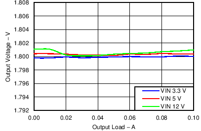
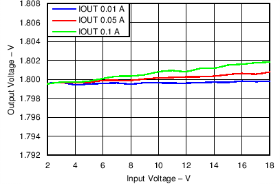
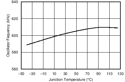
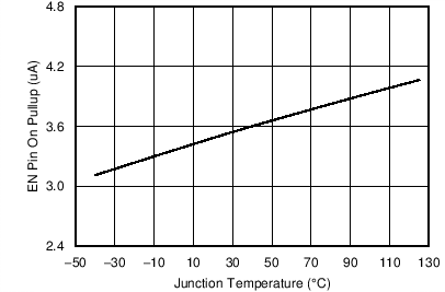
TA = 25°C, VIN = 12 V, VOUT1 = 1.2 V, VOUT2 = 1.8 V, VOUT3 = 3.3 V, ƒSW = 600 kHz (unless otherwise noted)
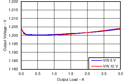
GUID-E7454FAD-DCA9-44F3-93B0-90488F8B5F02-low.png
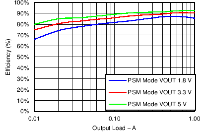
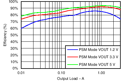
Figure 6-1 Buck1 Efficiency
GUID-7FEC2834-CDFE-4810-ADA0-A8F4BBC18E8C-low.png
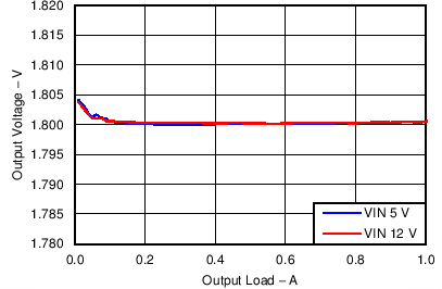
Figure 6-3 Buck1, Load Regulation
GUID-510DB435-BD87-4EEB-9591-B9251E1D1741-low.png
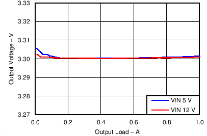
Figure 6-5 Buck3, Load Regulation
GUID-8B819B08-7FC6-4591-AE69-1C9FBFAF2274-low.png
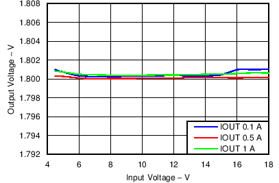
Figure 6-7 Buck2, Line Regulation
GUID-3C74C02C-2232-4A13-B958-212D97F8967F-low.png
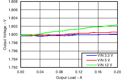
Figure 6-9 LDO1, Load Regulation
GUID-21998A0E-4247-48D8-855A-FCF516343DF0-low.png
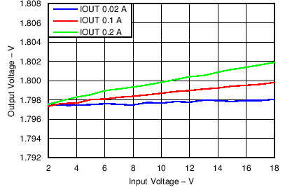
Figure 6-11 LDO1, Line Regulation
GUID-08E591AF-2019-4050-9081-17727A6A0D39-low.png
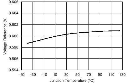
Figure 6-13 Voltage Reference vs Temperature
GUID-0DB2B082-FC90-472A-AA85-5F0F9EA248BA-low.png
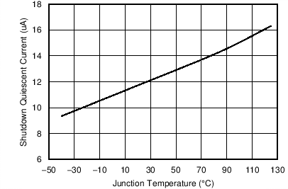
Figure 6-15 Shutdown Quiescent Current vs Temperature
GUID-105D8D43-4063-47CE-9FC2-0696C5E7D692-low.png
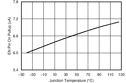
Figure 6-17 EN Pin Pullup Current vs Temperature, EN = 1.5 V
GUID-9034D235-C6F6-4088-84BC-67245D3A6B16-low.png
Figure 6-19 EN Pin Threshold Falling vs Temperature
GUID-CDC712FF-D834-4C09-9E94-C6A07C2D3D55-low.png
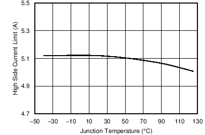
Figure 6-21 Buck1 High-Side Current Limit vs Temperature
GUID-61FD5191-847E-4838-9C0F-54B6EFDB96F6-low.png
Figure 6-2 Buck2 Efficiency
GUID-52F3FF6D-69B6-4045-A193-4CB082CD9FFA-low.png
Figure 6-4 Buck2, Load Regulation
GUID-A2ABD389-AEAD-4F0C-AD9A-ABB7B59FB5C5-low.png
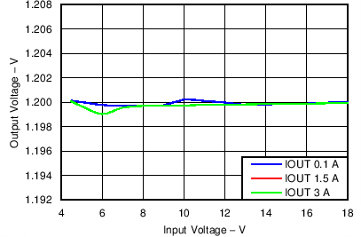
Figure 6-6 Buck1, Line Regulation
GUID-A5978751-2648-4C97-9E7A-175124CE1800-low.png
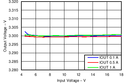
Figure 6-8 Buck3, Line Regulation
GUID-8F66B89E-76D5-41A0-B8A8-97EA8F61CB37-low.png
Figure 6-10 LDO2, Load Regulation
GUID-1BCCF0D1-4580-4AD3-8496-6A0F8B2236A2-low.png
Figure 6-12 LDO2, Line Regulation
GUID-194823F0-28EE-4A65-B7A4-44CD8AF05562-low.png
Figure 6-14 Oscillator Frequency vs Temperature
GUID-485FBF6F-2DE6-4EBB-8006-D4FC84F360B5-low.png
Figure 6-16 EN Pin Pullup Current vs Temperature, EN = 1 V
GUID-686327B3-6B67-4760-A9F8-841BE699DAB3-low.png
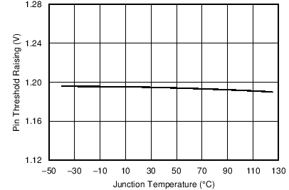
Figure 6-18 EN Pin Threshold Rising vs Temperature
GUID-6CF02DF3-8F59-4D8E-B80E-6BE38B041A95-low.png
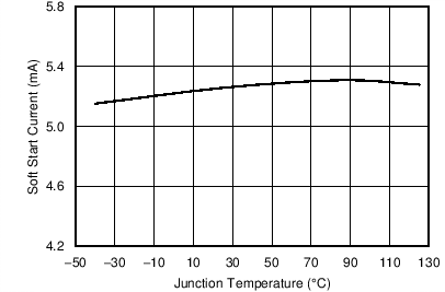
Figure 6-20 SS Pin Charge Current vs Temperature
GUID-59296FDF-9F85-4642-B285-0AFEA9ECA28D-low.png
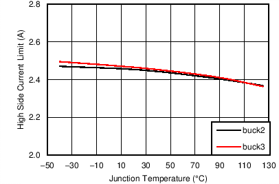
Figure 6-22 Buck2, 3 High-Side Current Limit vs Temperature