SLVSCF9D january 2014 – may 2023 TPS65262
PRODUCTION DATA
- 1
- 1 Features
- 2 Applications
- 3 Description
- 4 Revision History
- 5 Pin Configuration and Functions
- 6 Specifications
-
7 Detailed Description
- 7.1 Overview
- 7.2 Functional Block Diagram
- 7.3
Feature Description
- 7.3.1 Adjusting the Output Voltage
- 7.3.2 Enable and Adjusting Undervoltage Lockout
- 7.3.3 Soft-Start Time
- 7.3.4 Power-Up Sequencing
- 7.3.5 V7V Low Dropout Regulator and Bootstrap
- 7.3.6 Out-of-Phase Operation
- 7.3.7 Output Overvoltage Protection (OVP)
- 7.3.8 PSM
- 7.3.9 Slope Compensation
- 7.3.10 Overcurrent Protection
- 7.3.11 Power Good
- 7.3.12 Thermal Shutdown
- 7.4 Device Functional Modes
- 8 Application and Implementation
- 9 Device and Documentation Support
- 10Mechanical, Packaging, and Orderable Information
Package Options
Mechanical Data (Package|Pins)
- RHB|32
Thermal pad, mechanical data (Package|Pins)
- RHB|32
Orderable Information
7.3.3 Soft-Start Time
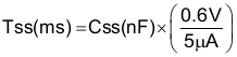
The voltage on the SS1 pin controls the start-up of buck1 output. When the voltage on the SS1 pin is less than the internal 0.6-V reference, The TPS65262 regulates the internal feedback voltage to the voltage on the SS1 pin instead of 0.6V, allowing VOUT to rise smoothly from 0V to its regulated voltage without inrush current. The device has an internal pull-up current source of 5µA (typical) that charges an external soft-start capacitor to provide a linear ramping voltage at SS1 pin.
Buck1’s soft-start time can be calculated approximately by Equation 4.
Buck2 and Buck3 have fixed 1-ms soft start time.
Equation 4.