SLVSDY9A March 2017 – November 2022 TPS65263-1Q1
PRODUCTION DATA
- 1 Features
- 2 Applications
- 3 Description
- 4 Revision History
- 5 Pin Configuration and Functions
- 6 Specifications
-
7 Detailed Description
- 7.1 Overview
- 7.2 Functional Block Diagram
- 7.3
Feature Description
- 7.3.1 Adjusting the Output Voltage
- 7.3.2 Enable and Adjusting UVLO
- 7.3.3 Soft-Start Time
- 7.3.4 Power-Up Sequencing
- 7.3.5 V7V Low-Dropout Regulator and Bootstrap
- 7.3.6 Out-of-Phase Operation
- 7.3.7 Output Overvoltage Protection (OVP)
- 7.3.8 PSM
- 7.3.9 Slope Compensation
- 7.3.10 Overcurrent Protection
- 7.3.11 Power Good
- 7.3.12 Thermal Shutdown
- 7.4 Device Functional Modes
- 7.5 Register Maps
- 8 Application and Implementation
- 9 Device and Documentation Support
- 10Mechanical, Packaging, and Orderable Information
Package Options
Mechanical Data (Package|Pins)
- RHB|32
Thermal pad, mechanical data (Package|Pins)
- RHB|32
Orderable Information
3 Description
The TPS65263-1Q1 incorporates triple-synchronous buck converters with 4.0- to 18-V wide input voltage. The converter with constant frequency peak current mode is designed to simplify its application while giving designers options to optimize the system according to targeted applications. The switching frequency of the converters is adjustable from 200 kHz to 2.3 MHz with an external resistor. 180° out-of-phase operation between buck1 and buck2, buck3 (buck2 and buck3 run in phase) minimizes the input filter requirements.
The initial start-up voltage of each buck can be set with external feedback resistors. The output voltage of buck2 can be dynamically scaled from 0.68 to 1.95 V in 10-mV steps with I2C-controlled 7 bits VID. The VID voltage transition slew rate is programmable with 3-bits control through I2C bus to optimize overshoot, undershoot during VID voltage transition.
Each buck in TPS65263-1Q1 can be I2C controlled for enabling and disabling output voltage, setting the pulse skipping mode (PSM) or forced continuous current (FCC) mode at light load condition and reading the power-good status, overcurrent warning, and die temperature warning.
The TPS65263-1Q1 features overvoltage, overcurrent, short-circuit, and overtemperature protection.
| PART NUMBER | PACKAGE | BODY SIZE (NOM) |
|---|---|---|
| TPS65263-1Q1 | RHB (VQFN, 32) | 5.00 mm × 5.00 mm |
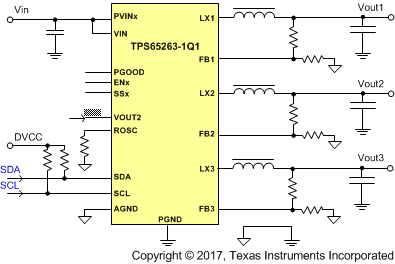
 Application Schematic
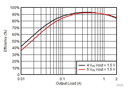
 Efficiency vs Output
Load