SLVSCS9D
december 2014 – may 2023
TPS65263-Q1
PRODUCTION DATA
1
1
Features
2
Applications
3
Description
4
Revision History
5
Pin Configuration and Functions
6
Specifications
6.1
Absolute Maximum Ratings
6.2
ESD Ratings
6.3
Recommended Operating Conditions
6.4
Thermal Information
6.5
Electrical Characteristics
6.6
Typical Characteristics
7
Detailed Description
7.1
Overview
7.2
Functional Block Diagram
7.3
Feature Description
7.3.1
Adjusting the Output Voltage
7.3.2
Enable and Adjusting UVLO
7.3.3
Soft-Start Time
7.3.4
Power-Up Sequencing
7.3.5
V7V Low-Dropout Regulator and Bootstrap
7.3.6
Out-of-Phase Operation
7.3.7
Output Overvoltage Protection (OVP)
7.3.8
PSM
7.3.9
Slope Compensation
7.3.10
Overcurrent Protection
7.3.10.1
High-Side MOSFET Overcurrent Protection
7.3.10.2
Low-Side MOSFET Overcurrent Protection
7.3.11
Power Good
7.3.11.1
Adjustable Switching Frequency
7.3.12
Thermal Shutdown
7.4
Device Functional Modes
7.4.1
Serial Interface Description
7.4.2
I2C Update Sequence
7.5
Register Maps
7.5.1
VOUT2_SEL: Vout2 Voltage Selection Register (Address = 0x01H)
7.5.2
VOUT1_COM: Buck1 Command Register (offset = 0x03H)
7.5.3
VOUT2_COM: Buck2 Command Register (offset = 0x04H)
7.5.4
VOUT3_COM: Buck3 Command Register (offset = 0x05H)
7.5.5
SYS_STATUS: System Status Register (offset = 0x06H)
8
Application and Implementation
8.1
Application Information
8.2
Typical Application
8.2.1
Design Requirements
8.2.2
Detailed Design Procedure
8.2.2.1
Output Inductor Selection
8.2.2.2
Output Capacitor Selection
8.2.2.3
Input Capacitor Selection
8.2.2.4
Loop Compensation
8.2.3
Application Curves
8.3
Power Supply Recommendations
8.4
Layout
8.4.1
Layout Guidelines
8.4.2
Layout Example
9
Device and Documentation Support
9.1
Receiving Notification of Documentation Updates
9.2
Support Resources
9.3
Trademarks
9.4
Electrostatic Discharge Caution
9.5
Glossary
10
Mechanical, Packaging, and Orderable Information
Package Options
Mechanical Data (Package|Pins)
RHB|32
MPQF130D
Thermal pad, mechanical data (Package|Pins)
RHB|32
QFND029X
Orderable Information
slvscs9d_oa
slvscs9d_pm
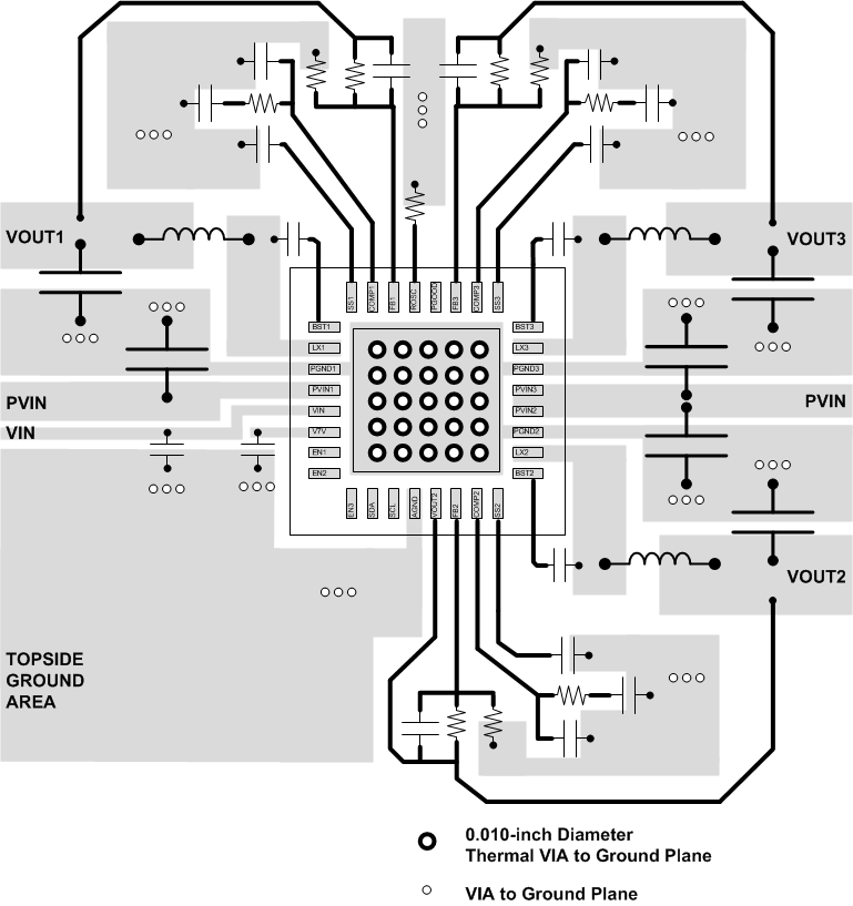
8.4.2
Layout Example
Figure 8-25
PCB Layout