SLVSCN0C june 2014 – may 2023 TPS65263
PRODUCTION DATA
- 1
- 1 Features
- 2 Applications
- 3 Description
- 4 Revision History
- 5 Device Comparison Table
- 6 Pin Configuration and Functions
- 7 Specifications
-
8 Detailed Description
- 8.1 Overview
- 8.2 Functional Block Diagram
- 8.3
Feature Description
- 8.3.1 Adjusting the Output Voltage
- 8.3.2 Enable and Adjusting UVLO
- 8.3.3 Soft-Start Time
- 8.3.4 Power-Up Sequencing
- 8.3.5 V7V Low Dropout Regulator and Bootstrap
- 8.3.6 Out-of-Phase Operation
- 8.3.7 Output Overvoltage Protection (OVP)
- 8.3.8 Pulse Skipping Mode (PSM)
- 8.3.9 Slope Compensation
- 8.3.10 Overcurrent Protection
- 8.3.11 Power Good
- 8.3.12 Thermal Shutdown
- 8.4 Device Functional Modes
- 8.5
Register Maps
- 8.5.1 Register Description
- 8.5.2 VOUT1_SEL: Vout1 Voltage Selection Register (offset = 0x00H)
- 8.5.3 VOUT2_SEL: Vout2 Voltage Selection Register (offset = 0x01H)
- 8.5.4 VOUT3_SEL: Vout3 Voltage Selection Register (offset = 0x02H)
- 8.5.5 VOUT1_COM: Buck1 Command Register (offset = 0x03H)
- 8.5.6 VOUT2_COM: Buck2 Command Register (offset = 0x04H)
- 8.5.7 VOUT3_COM: Buck3 Command Register (offset = 0x05H)
- 8.5.8 SYS_STATUS: System Status Register (offset = 0x06H)
- 9 Application and Implementation
- 10Device and Documentation Support
- 11Mechanical, Packaging, and Orderable Information
Package Options
Mechanical Data (Package|Pins)
- RHB|32
Thermal pad, mechanical data (Package|Pins)
- RHB|32
Orderable Information
9.2.3 Application Curves
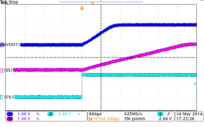 Figure 9-2 BUCK1, Soft-Start, Iout = 3 A
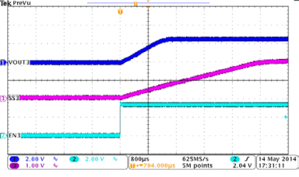 Figure 9-4 BUCK3, Soft-Start, Iout = 2 A
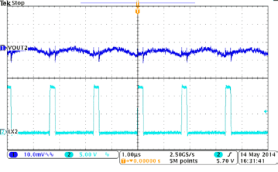 Figure 9-6 BUCK2, Output Voltage Ripple, Iout = 3 A
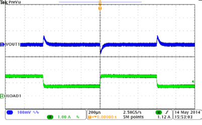 Figure 9-8 BUCK1, Load Transient, 0.75 to 1.5 A SR = 0.25 A/µs
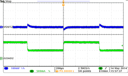 Figure 9-10 BUCK2, Load Transient, 0.5 to 1 A SR = 0.25 A/µs
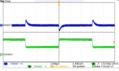 Figure 9-12 BUCK3, Load Transient, 0.5 to 1 A SR = 0.25 A/µs
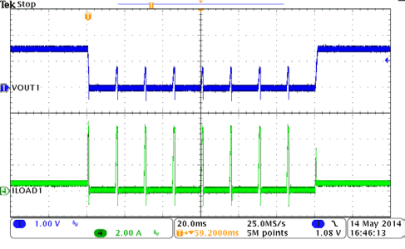 Figure 9-14 BUCK1, Hiccup and Recovery
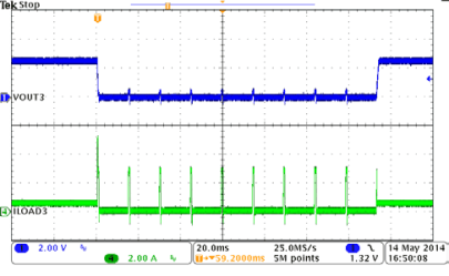 Figure 9-16 BUCK3, Hiccup and Recovery
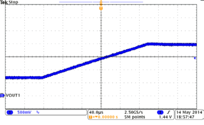 Figure 9-18 VID1 from 00 to 7F, SR = 10 mV/cycle
 Figure 9-20 VID2 from 00 to 7F, SR =
10 mV/cycle
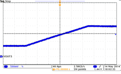 Figure 9-22 VID3 from 00 to 7F, SR = 10 mV/cycle
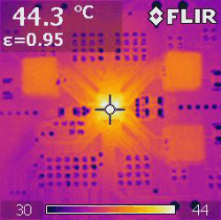
| VIN = 12 V; VOUT1 = 1.5 V / 1.5 A; VOUT2 = 1.2 V / 1 A | ||
| VOUT3 = 2.5 V / 1 A | TA = 26.8°C | |
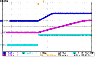 Figure 9-3 BUCK2, Soft-Start, Iout = 2 A
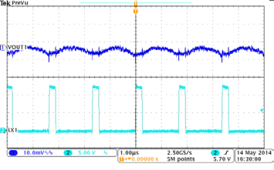 Figure 9-5 BUCK1, Output Voltage Ripple, Iout = 3 A
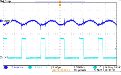 Figure 9-7 BUCK3, Output Voltage Ripple, Iout = 2 A
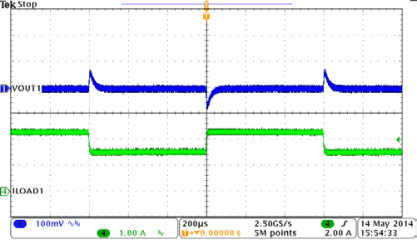 Figure 9-9 BUCK1, Load Transient, 1.5 to 2.25 A SR = 0.25 A/µs
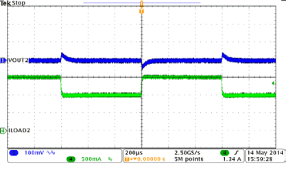 Figure 9-11 BUCK2, Load Transient, 1 to 1.5 A SR = 0.25 A/µs
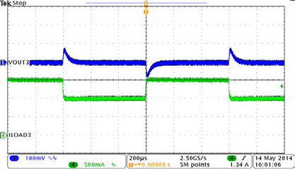 Figure 9-13 BUCK3, Load Transient, 1 to 1.5 A SR = 0.25 A/µs
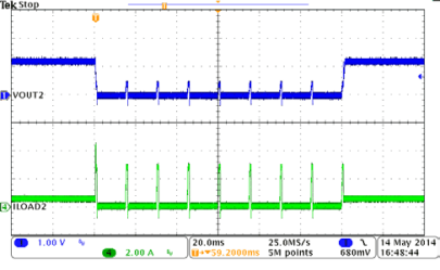 Figure 9-15 BUCK2, Hiccup and Recovery
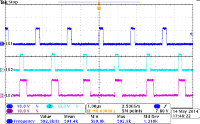 Figure 9-17 180° Out-of-Phase
 Figure 9-19 VID1 from 7F to 00, SR = 10 mV/cycle
 Figure 9-21 VID2 from 7F to 00, SR = 10 mV/cycle
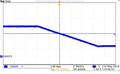 Figure 9-23 VID3 from 7F to 00, SR = 10 mV/cycle
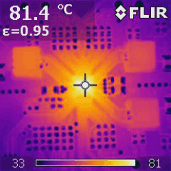
| VIN = 12 V; VOUT1 = 1.5 V / 3 A; VOUT2 = 1.2 V / 2 A | ||
| VOUT3 = 2.5 V / 2 A | TA = 26.8°C | |