-
TPS65266 2.7- to 6.5-V Input Voltage, 3-A/2-A/2-A Output Current Triple Synchronous Step-Down Converter
- 1 Features
- 2 Applications
- 3 Description
- 4 Revision History
- 5 Pin Configuration and Functions
- 6 Specifications
-
7 Detailed Description
- 7.1 Overview
- 7.2 Functional Block Diagram
- 7.3
Feature Description
- 7.3.1 Adjusting the Output Voltage
- 7.3.2 Enable and Adjusting UVLO
- 7.3.3 Soft-Start Time
- 7.3.4 Power-Up Sequencing
- 7.3.5 Boostrap Voltage and BST-LX UVLO
- 7.3.6 Out of Phase Operation
- 7.3.7 Output Overvoltage Protection (OVP)
- 7.3.8 Slope Compensation
- 7.3.9 Overcurrent Protection
- 7.3.10 Power Good
- 7.3.11 Adjustable Switching Frequency
- 7.3.12 Thermal Shutdown
- 7.4 Device Functional Modes
- 8 Application and Implementation
- 9 Power Supply Recommendations
- 10Layout
- 11Device and Documentation Support
- 12Mechanical, Packaging, and Orderable Information
- IMPORTANT NOTICE
Package Options
Mechanical Data (Package|Pins)
- RHB|32
Thermal pad, mechanical data (Package|Pins)
- RHB|32
Orderable Information
TPS65266 2.7- to 6.5-V Input Voltage, 3-A/2-A/2-A Output Current Triple Synchronous Step-Down Converter
1 Features
- Operating Input Voltage Range 2.7 to 6.5 V
- Feedback Reference Voltage 0.6 V ±1%
- Maximum Continuous Output Current 3 A/2 A/2 A
- Dedicated Enable and Soft Start
- Accurate Start-Up Timing Control With Enable Pins Discharge
- Forced Continuous Current (FCC) Mode at Light Load
- Cycle-by-Cycle Current Limiting With Hiccup Mode Overcurrent Protection
- Adjustable Clock Frequency 250 kHz to 2.4 MHz
- External Clock Synchronization
- Power-Good Indicator
- Overtemperature Protection
2 Applications
- Printer and Scanner
- Digital TV
- Set Top Box
- Home Gateway and Access Point Networks
- Surveillance
3 Description
The TPS65266 incorporates 3 channels of high-efficiency synchronous buck converter for applications operating off the adaptor or battery with input voltage lower than 6.5 V.
The buck DC/DC converter integrates power MOSFETs for optimized power efficiency and reduces external component counts. The peak current mode control simplifies the compensation and fast transient response. High clock frequency allows smaller and low-value inductors and capacitors. External compensation supports optimized loop compensation and fast transient response. In light load condition, the buck converter operates in FCC mode for a reduction in noise susceptibility and RF interference. Cycle-by-cycle overcurrent limiting with hiccup mode limits MOSFET power dissipation in short circuit or overloading fault conditions.
The TPS65266 features a power-good supervisor circuit that monitors all converter outputs. The PGOOD pin is asserted after the output voltages in each channel are in regulation and sequencing is done.
When continuous heavy overload or short circuit increases power dissipation in the buck converter, internal thermal protection circuit shuts off the device to prevent damage. Recovery from a thermal shutdown is automatic after the device has cooled sufficiently.
Device Information(1)
| PART NUMBER | PACKAGE | BODY SIZE (NOM) |
|---|---|---|
| TPS65266 | VQFN (32) | 5.00 mm × 5.00 mm |
- For all available packages, see the orderable addendum at the end of the data sheet.
Simplified Application Schematic

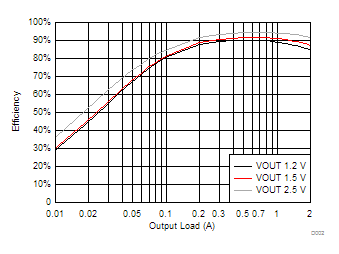
Efficiency vs Output Load

5 Pin Configuration and Functions
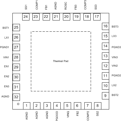
Pin Functions
| PIN | DESCRIPTION | |
|---|---|---|
| NO. | NAME | |
| 1 | AGND | Analog ground pin |
| 2 | AGND | Analog ground pin |
| 3 | AGND | Analog ground pin |
| 4 | PGOOD | An open-drain output; asserts low if output voltage of bucks beyond regulation range due to thermal shutdown, over-current, under-voltage, or ENx low. |
| 5 | VINQ | Input voltage of converter controller and reference power supply bias. TI recommends to connect a 1-µF capacitor from the pin to analog ground and put the capacitor as near as possible to this pin. |
| 6 | FB2 | Feedback Kelvin sensing pin for buck2 output voltage. Connect this pin to buck2 feedback resistor divider. |
| 7 | COMP2 | Error amplifier output and loop compensation pin for buck2. Connect a series resistor and capacitor to compensate the control loop of buck converter 2 with peak current PWM mode. |
| 8 | SS2 | Soft-start and tracking input for buck2 converter. An internal 5.5-µA pullup current source is connected to this pin. The soft-start time of buck2 can be programmed by connecting a capacitor between this pin and ground. |
| 9 | BST2 | Boot strapped supply to the high-side floating gate driver in buck2 converter. Connect a capacitor (47 nF recommended) from BST2 pin to LX2 pin. |
| 10 | LX2 | Switching node connection to the inductor and bootstrap capacitor for buck2 converter. The voltage swing at this pin is from a diode voltage below the ground up to VIN2 voltage. |
| 11 | PGND2 | Power ground connection of buck2. Connect PGND2 pin as close as practical to the (–) terminal of VIN2 input ceramic capacitor. |
| 12 | VIN2 | Input power supply for buck2. Connect VIN2 pin as close as practical to the (+) terminal of an input ceramic capacitor (10 µF suggested). |
| 13 | VIN3 | Input power supply for buck3. Connect VIN3 pin as close as practical to the (+) terminal of an input ceramic capacitor (10 µF suggested). |
| 14 | PGND3 | Power ground connection of buck3. Connect PGND3 pin as close as practical to the (–) terminal of VIN3 input ceramic capacitor. |
| 15 | LX3 | Switching node connection to the inductor and bootstrap capacitor for buck3 converter. The voltage swing at this pin is from a diode voltage below the ground up to VIN3 voltage. |
| 16 | BST3 | Boot strapped supply to the high-side floating gate driver in buck3 converter. Connect a capacitor (47 nF recommended) from BST3 pin to LX3 pin. |
| 17 | SS3 | Soft-start and tracking input for buck3 converter. An internal 5.5-µA pullup current source is connected to this pin. The soft-start time of buck3 can be programmed by connecting a capacitor between this pin and ground. |
| 18 | COMP3 | Error amplifier output and loop compensation pin for buck3. Connect a series resistor and capacitor to compensate the control loop of buck converter 3 with peak current PWM mode. |
| 19 | FB3 | Feedback Kelvin sensing pin for buck3 output voltage. Connect this pin to buck3 feedback resistor divider. |
| 20 | ROSC | Oscillator frequency programmable pin. Connect an external resistor to set the switching frequency. |
| 21 | AGND | Analog ground common to buck controllers and other analog circuits. It must be routed separately from high-current power grounds to the (–) terminal of bypass capacitor of input voltage VINQ. |
| 22 | FB1 | Feedback Kelvin sensing pin for buck1 output voltage. Connect this pin to buck1 feedback resistor divider. |
| 23 | COMP1 | Error amplifier output and loop compensation pin for buck1. Connect a series resistor and capacitor to compensate the control loop of buck converter 1 with peak current PWM mode. |
| 24 | SS1 | Soft-start and tracking input for buck1 converter. An internal 5.5-µA pullup current source is connected to this pin. The soft-start time of buck1 can be programmed by connecting a capacitor between this pin and ground. |
| 25 | BST1 | Boot strapped supply to the high-side floating gate driver in buck1 converter. Connect a capacitor (47 nF recommended) from BST1 pin to LX1 pin. |
| 26 | LX1 | Switching node connection to the inductor and bootstrap capacitor for buck1 converter. The voltage swing at this pin is from a diode voltage below the ground up to VIN1 voltage. |
| 27 | PGND1 | Power ground connection of buck1. Connect PGND1 pin as close as practical to the (–) terminal of VIN1 input ceramic capacitor. |
| 28 | VIN1 | Input power supply for buck1. Connect VIN1 pin as close as practical to the (+) terminal of an input ceramic capacitor (suggest 10 µF). |
| 29 | EN1 | Enable for buck1 converter. Float to enable. Can use this pin to adjust the input undervoltage lockup of buck1 with resistors divider. |
| 30 | EN2 | Enable for buck2 converter. Float to enable. Can use this pin to adjust the input undervoltage lockup of buck2 with resistors divider. |
| 31 | EN3 | Enable for buck3 converter. Float to enable. Can use this pin to adjust the input undervoltage lockup of buck3 with resistors divider. |
| 32 | GND | Ground pin |
| — | Thermal PAD | No electric connection to any signal. Soldered to the ground in PCB for better thermal performance. |
6 Specifications
6.1 Absolute Maximum Ratings
over operating free-air temperature (unless otherwise noted) (1)| MIN | MAX | UNIT | ||
|---|---|---|---|---|
| Voltage at | VIN1, VIN2, VIN3, VINQ | –0.3 | 7 | V |
| LX1, LX2, LX3 (maximum withstand voltage transient <20 ns) | –1.0 | 7 | ||
| BST1, BST2, BST3 referenced to LX1, LX2, LX3 pins respectively | –0.3 | 7 | ||
| EN1, EN2, EN3, PGOOD | –0.3 | 7 | ||
| FB1, FB2, FB3, COMP1 , COMP2, COMP3, SS1, SS2, SS3, ROSC | –0.3 | 3.6 | ||
| AGND, PGND1, PGND2, PGND3 | –0.3 | 0.3 | ||
| TJ | Operating junction temperature | –40 | 150 | °C |
| Tstg | Storage temperature | –55 | 150 | °C |
6.2 ESD Ratings
| VALUE | UNIT | |||
|---|---|---|---|---|
| V(ESD) | Electrostatic discharge | Human body model (HBM), per ANSI/ESDA/JEDEC JS-001, all pins(1) | ±2000 | V |
| Charged device model (CDM), per JEDEC specification JESD22-C101, all pins(2) | ±500 | |||
6.3 Recommended Operating Conditions
over operating free-air temperature range (unless otherwise noted)| MIN | MAX | UNIT | ||
|---|---|---|---|---|
| Voltage at | VIN1, VIN2, VIN3, VINQ | 2.7 | 6.5 | V |
| LX1, LX2, LX3 (maximum withstand voltage transient <20 ns) | –0.8 | 6.5 | ||
| BST1, BST2, BST3 referenced to LX1, LX2, LX3 pins respectively | –0.1 | 6.5 | ||
| EN1, EN2, EN3, PGOOD | –0.1 | 6.5 | ||
| FB1, FB2, FB3, COMP1 , COMP2, COMP3, SS1, SS2, SS3, ROSC | –0.1 | 3 | ||
| TJ | Operating junction temperature | –40 | 125 | °C |
6.4 Thermal Information
| THERMAL METRIC(1) | TPS65266 | UNIT | |
|---|---|---|---|
| RHB | |||
| 32 PINS | |||
| RθJA | Junction-to-ambient thermal resistance | 34.2 | °C/W |
| RθJC(top) | Junction-to-case (top) thermal resistance | 27.5 | |
| RθJB | Junction-to-board thermal resistance | 8.3 | |
| ψJT | Junction-to-top characterization parameter | 0.4 | |
| ψJB | Junction-to-board characterization parameter | 8.3 | |
| RθJC(bot) | Junction-to-case (bottom) thermal resistance | 2.8 | |
6.5 Electrical Characteristics
TA = 25°C, VIN = 5 V, FSW = 1 MHz (unless otherwise noted)| PARAMETER | TEST CONDITIONS | MIN | TYP | MAX | UNIT | |
|---|---|---|---|---|---|---|
| INPUT SUPPLY VOLTAGE | ||||||
| VIN | Input voltage range | 2.7 | 6.5 | V | ||
| UVLO | VIN undervoltage lockout | VIN rising | 2.35 | 2.45 | 2.6 | V |
| VIN falling | 2.15 | 2.25 | 2.35 | V | ||
| Hysteresis | 200 | mV | ||||
| IDDSDN | Shutdown supply current | EN1 = EN2 = EN3 = 0 V | 9 | µA | ||
| IDDQ_NSW | Input quiescent current without buck1/2/3 switching | EN1 = EN2 = EN3 = 5 V, FB1 = FB2 = FB3 = 0.8 V |
790 | µA | ||
| IDDQ_NSW1 | EN1 = 5 V, EN2 = EN3 = 0 V, FB1 = 0.8 V |
340 | µA | |||
| IDDQ_NSW2 | EN2 = 5 V, EN1 = EN3 = 0 V, FB2 = 0.8 V |
340 | µA | |||
| IDDQ_NSW3 | EN3 = 5 V, EN1 = EN2 = 0 V, FB3 = 0.8 V |
340 | µA | |||
| BUCK1, BUCK2, BUCK3 | ||||||
| VFB | Feedback voltage | VCOMP = 1.2 V | 0.594 | 0.6 | 0.606 | V |
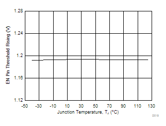
| VENXH | EN1/2/3 high-level input voltage | 1.2 | 1.26 | V | ||
| VENXL | EN1/2/3 low-level input voltage | 1.1 | 1.15 | V | ||
| IENX1 | EN1/2/3 pullup current | ENx = 1 V | 1.8 | 2.1 | 2.4 | µA |
| IENX2 | EN1/2/3 pullup current | ENx = 1.3 V | 5.3 | µA | ||
| IENhys | Hysteresis current | 3.2 | µA | |||
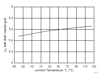
| ISSX | Soft-start charging current | 4.5 | 5.5 | 6.5 | µA | |
| tON_MIN | Minimum on-time | 80 | 100 | ns | ||
| Gm_EA | Error amplifier transconductance | –2 µA < ICOMPX < 2 µA | 290 | µS | ||
| Gm_PS1/2/3 | COMP1/2/3 voltage to inductor current Gm(1) | ILX = 0.5 A | 10 | A/V | ||
| ILIMIT1 | Buck1 peak inductor current limit | 3.9 | 4.6 | 5.3 | A | |
| ILIMITSINK1 | Buck1 low-side sink current limit | 1.4 | ||||
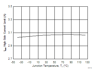
| ILIMIT2/3 | Buck2/3 peak inductor current limit | 2.5 | 3.1 | 3.7 | A | |
| ILIMITSINK2/3 | Buck2/3 low-side sink current limit | 1.2 | A | |||
| Rdson_HS1 | Buck1 high-side switch resistance | VINQ = 5 V | 45 | mΩ | ||
| Rdson_LS1 | Buck1 low-side switch resistance | VINQ = 5 V | 50 | mΩ | ||
| Rdson_HS2 | Buck2 high-side switch resistance | VINQ = 5 V | 60 | mΩ | ||
| Rdson_LS2 | Buck2 low-side switch resistance | VINQ = 5 V | 60 | mΩ | ||
| Rdson_HS3 | Buck3 high-side switch resistance | VINQ = 5 V | 60 | mΩ | ||
| Rdson_LS3 | Buck3 low-side switch resistance | VINQ = 5 V | 60 | mΩ | ||
| HICCUP TIMING | ||||||
| tHiccup_wait | Overcurrent wait time(1) | 512 | cycles | |||
| tHiccup_re | Hiccup time before restart(1) | 16382 | cycles | |||
| POWER GOOD | ||||||
| Vth_PG | Feedback voltage threshold | FBx undervoltage falling | 92.5 | %VREF | ||
| FBx undervoltage rising | 95 | %VREF | ||||
| tDEGLITCH(PG)_F | PGOOD falling edge deglitch time | 128 | cycles | |||
| tRDEGLITCH(PG)_R | PGOOD rising edge deglitch time | 16350 | cycles | |||
| IPG | PGOOD pin leakage | 1 | µA | |||
| VLOW_PG | PGOOD pin low voltage | ISINK = 1 mA | 0.4 | V | ||
| OSCILLATOR | ||||||
| FSW | Switching frequency | ROSC = 51.1 kΩ | 920 | 1000 | 1080 | kHz |
| FSW_range | Switching frequency | 250 | 2400 | kHz | ||
| FSYNC | Clock sync frequency range | 250 | 2400 | kHz | ||
| tSYNC_w | Clock sync minimum pulse duration | 80 | ns | |||
| FSYNC_HI | Clock sync high threshold | 2 | V | |||
| VSYNC_LO | Clock sync low threshold | 0.4 | V | |||
| THERMAL PROTECTION | ||||||
| TTRIP_OTP(1) | Thermal protection trip point | Temperature rising | 160 | °C | ||
| THYST_OTP(1) | Hysteresis | 20 | °C | |||
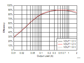
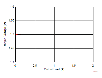
6.6 Typical Characteristics
TA = 25°C, VIN = 5 V, VOUT1 = 1.0 V, VOUT2 = 1.5 V, VOUT3 = 1.8 V FSW = 1 MHz (unless otherwise noted)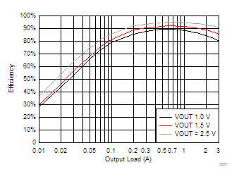
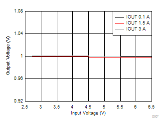
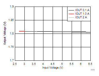
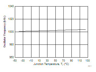
| ROSC = 51.1 kΩ | ||
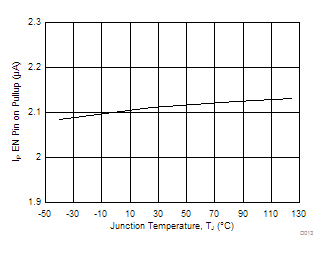
| VIN = 5 V | EN = 1 V | |
| VIN = 5 V | ||
| VIN = 5 V | ||
| VIN = 5 V | ||
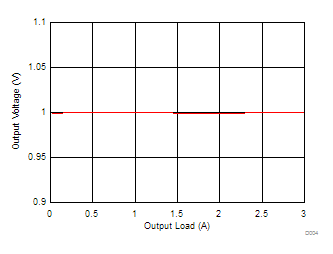
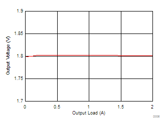
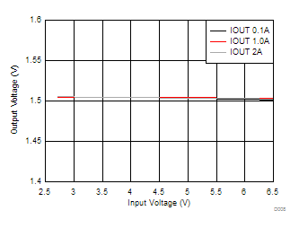
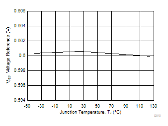
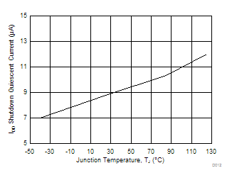
| VIN = 5 V | ||
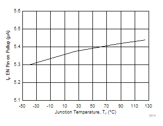
| VIN = 5 V | EN = 1.3 V | |
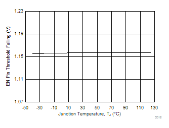
| VIN = 5 V | ||
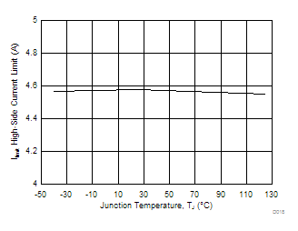
| VIN = 5 V | ||

| VIN = 5 V | ||
7 Detailed Description
7.1 Overview
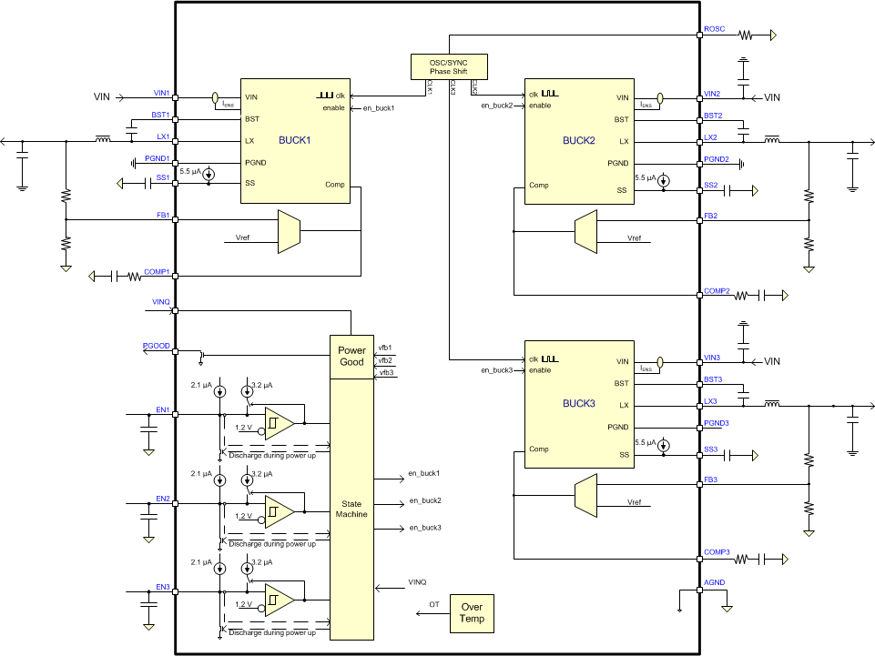
The TPS65266 is a triple 3-A/2-A/2-A output current, synchronous step-down (buck) converter for applications operating off the adaptor or battery with input voltage lower than 6.5 V. The feedback voltage reference for each buck is 0.6 V. Each buck is independent with dedicated enable, soft-start, and loop compensation. The TPS65266 implements a constant frequency, peak current mode control that simplifies external loop compensation. The switch clock of buck1 is 180° out-of-phase operation from the clock of buck2 and buck3 channels to reduce input current ripple, input capacitor size and power-supply-induced noise.
The TPS65266 has been designed for safe monotonic startup into prebiased loads. The default start-up is when VIN is typically 2.45 V. The ENx pin has an internal pullup current source that can be used to adjust the input voltage undervoltage lockout (UVLO) with two external resistors. In addition, the EN pin can be floating for automatically starting up the converters with the internal pullup current.
The TPS65266 features PGOOD pin to supervise output voltages of buck converter. The TPS65266 has power-good comparators with hysteresis, which monitor the output voltages through internal feedback voltages. When all bucks are in regulation range and power sequence is done, PGOOD is asserted high.
The SS (soft-start/tracking) pin is used to minimize inrush currents or provide power-supply sequencing during power up. A small-value capacitor or resistor divider should be coupled to the pin for soft start or critical power-supply sequencing requirements.
The TPS65266 is protected from overload and thermal fault conditions.
7.2 Functional Block Diagram
7.3 Feature Description
7.3.1 Adjusting the Output Voltage
The output voltage of each buck is set with a resistor divider from the output of buck to the FB pin. TI recommends to use 1% tolerance or better resistors.
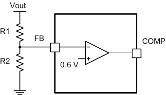 Figure 21. Voltage Divider Circuit

To improve efficiency at light loads, consider using larger-value resistors. If the values are too high, the regulator is more sensitive to noise. Table 1 shows the recommended resistor values.
Table 1. Output Resistor Divider Selection
| Output Voltage (V) |
R1 (kΩ) |
R2 (kΩ) |
|---|---|---|
| 1 | 10 | 15 |
| 1.2 | 10 | 10 |
| 1.5 | 15 | 10 |
| 1.8 | 20 | 10 |
| 2.5 | 31.6 | 10 |
| 3.3 | 45.3 | 10 |
| 3.3 | 22.6 | 4.99 |
| 5 | 73.2 | 10 |
| 5 | 36.5 | 4.99 |
7.3.2 Enable and Adjusting UVLO
The EN1/2/3 pin provides electrical on and off control of the device. After the EN1/2/3 pin voltage exceeds the threshold voltage, the device starts operation. If each ENx pin voltage is pulled below the threshold voltage, the regulator stops switching and enters low Iq state.
The EN pin has an internal pullup current source, allowing the user to float the EN pin for enabling the device. If an application requires controlling the EN pin, use open-drain or open-collector output logic to interface with the pin.
The device implements internal UVLO circuitry on the VINQ pin. The device is disabled when the VINQ pin voltage falls below the internal VIN UVLO threshold. The internal VIN UVLO threshold has a hysteresis of 200 mV. If an application requires either a higher UVLO threshold on the VINQ pin or a secondary UVLO on the VINx, in split-rail applications, then the ENx pin can be configured as shown in Figure 22, Figure 23, and Figure 24. When using the external UVLO function, TI recommends to set the hysteresis to be >200 mV.
The EN pin has a small pullup current Ip, which sets the default state of the pin to enable when no external components are connected. The pullup current is also used to control the voltage hysteresis for the UVLO function because it increases by Ih after the EN pin crosses the enable threshold. Calculate the UVLO thresholds using Equation 2 and Equation 3.


where
- Ih = 3.2 µA
- Ip = 2.1 µA
- VENRISING = 1.2 V
- VENFALLING = 1.15 V
 Figure 22. Adjustable VINQ UVLO
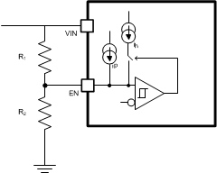 Figure 23. Adjustable VIN UVLO, VINQ > 2.7 V
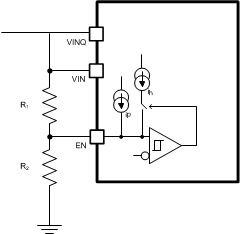 Figure 24. Adjustable VIN and VINQ UVLO
7.3.3 Soft-Start Time
The voltage on the respective SS pin controls the start-up of buck output. When the voltage on the SS pin is less than the internal 0.6-V reference, the TPS65266 regulates the internal feedback voltage to the voltage on the SS pin instead of 0.6 V. The SS pin can be used to program an external soft-start function or to allow output of buck to track another supply during start-up. The device has an internal pullup current source of 5.5 μA (typical) that charges an external soft-start capacitor to provide a linear ramping voltage at SS pin. The TPS65266 regulates the internal feedback voltage to the voltage on the SS pin, allowing VOUT to rise smoothly from 0 V to its regulated voltage without inrush current. Calculate the approximate soft-start time with Equation 4.

Many of the common power-supply sequencing methods can be implemented using the SSx and ENx pins. Figure 25 shows the method implementing ratiometric sequencing by connecting the SSx pins of three buck channels together. The regulator outputs ramp up and reach regulation at the same time. When calculating the soft-start time, the pullup current source must be tripled in Equation 4.
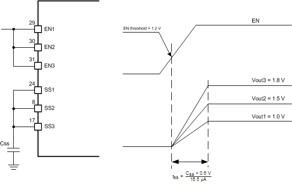 Figure 25. Ratiometric Power-Up Using SSx Pins
Simultaneous power-supply sequencing can be implemented by connecting capacitor to SSx pin, shown in Figure 26. Using Equation 4 and Equation 5, calculate the capacitors.

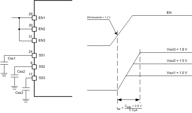 Figure 26. Simultaneous Startup Sequence Using SSx Pins
7.3.4 Power-Up Sequencing
The TPS65266 has a dedicated enable pin and soft-start pin for each converter. The converter enable pins are biased by a current source that allows for easy sequencing by the addition of an external capacitor. Enable pins have a discharge function, which ensures power-up sequencing is effective at quickly powering down and up status. Disabling the converter with an active pulldown transistor on the ENs pin allows for a predictable power-down timing operation. Figure 27 shows the timing diagram of a typical buck power-up sequence with connecting a capacitor at ENx pin.
When VINQ pin voltage rises to about 1 V, the internal EN turns on and a typical 1.4-µA current is charging ENx pin from input supply. If any of the EN pin voltages reaches 0.5 V when powered up, three EN pin discharge functions are triggered and keep 2 ms with discharge resistor around 1.2 kΩ to GND, then a 2.1-µA pullup current is sourcing ENx. After ENx pin voltage reaches to ENx enabling threshold, 3.2-µA hysteresis current sources to the pin to improve noise sensitivity.
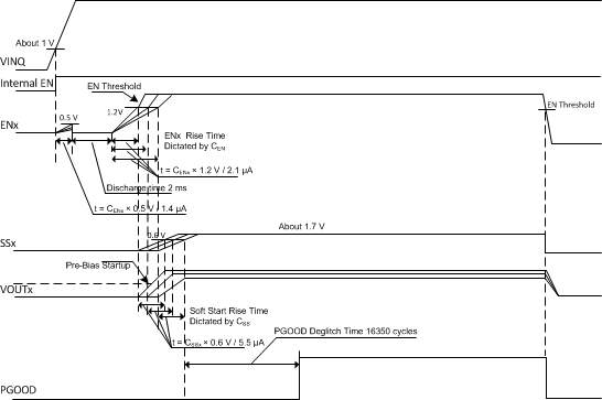 Figure 27. Startup Power Sequence
7.3.5 Boostrap Voltage and BST-LX UVLO
Each high-side MOSFET driver is biased from the floating bootstrap capacitor, CB, shown in Figure 28, which is normally recharged during each cycle through an internal low-side MOSFET or the body diode of a low-side MOSFET when the high-side MOSFET turns off. The boot capacitor is charged when the BST pin voltage is less than VIN and BST-LX voltage is below regulation. The recommended value of this ceramic capacitor is 47 nF. TI recommends a ceramic capacitor with an X7R- or X5R-grade dielectric with a voltage rating of 10 V or higher because of the stable characteristics over temperature and voltage.
To improve dropout, the device is designed to operate at 100% duty cycle as long as the BST to LX pin voltage is greater than the BST-LX UVLO threshold, which is typically 2.1 V. When the voltage between BST and LX drops below the BST-LX UVLO threshold, the high-side MOSFET is turned off and the low-side MOSFET is turned on allowing the boot capacitor to be recharged.
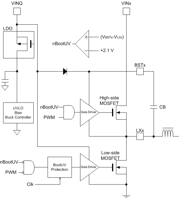 Figure 28. Bootstrap Voltage and Diagram
7.3.6 Out of Phase Operation
To reduce input ripple current, the switch clock of buck1 is 180° out-of-phase from the clock of buck2 and buck3. This enables the system by having less input current ripple to reduce input capacitors’ size, cost, and EMI.
7.3.7 Output Overvoltage Protection (OVP)
The device incorporates an OVP circuit to minimize output voltage overshoot. When the output is overloaded, the error amplifier compares the actual output voltage to the internal reference voltage. If the FB pin voltage is lower than the internal reference voltage for a considerable time, the output of the error amplifier demands maximum output current. After the condition is removed, the regulator output rises and the error amplifier output transitions to the steady-state voltage. In some applications with small output capacitance, the load can respond faster than the error amplifier. This leads to the possibility of an output overshoot. Each buck compares the FB pin voltage to the OVP threshold. If the FB pin voltage is greater than the OVP threshold, the high-side MOSFET is turned off preventing current from flowing to the output and minimizing output overshoot. When the FB voltage drops lower than the OVP threshold, the high-side MOSFET turns on at the next clock cycle.
7.3.8 Slope Compensation
To prevent the subharmonic oscillations when the device operates at duty cycles greater than 50%, the TPS65266 adds built-in slope compensation, which is a compensating ramp to the switch current signal.
7.3.9 Overcurrent Protection
The device is protected from overcurrent conditions by cycle-by-cycle current limiting on both the high-side MOSFET and low-side MOSFET.
7.3.9.1 High-Side MOSFET Overcurrent Protection
The device implements current mode control, which uses the COMP pin voltage to control the turn off of the high-side MOSFET and the turn-on of the low-side MOSFET on a cycle-by-cycle basis. Each cycle the switch current and the current reference generated by the COMP pin voltage are compared, when the peak switch current intersects the current reference, the high-side switch is turned off.
7.3.9.2 Low-Side MOSFET Overcurrent Protection
While the low-side MOSFET is turned on, its conduction current is monitored by the internal circuitry. During normal operation the low-side MOSFET sources current to the load. At the end of every clock cycle, the low-side MOSFET sourcing current is compared to the internally set low-side sourcing current limit. If the low-side sourcing current is exceeded, the high-side MOSFET is not turned on and the low-side MOSFET stays on for the next cycle. The high-side MOSFET is turned on again when the low-side current is below the low-side sourcing current limit at the start of a cycle.
The low-side MOSFET may also sink current from the load. If the low-side sinking current limit is exceeded, the low-side MOSFET is turned off immediately for the rest of that clock cycle. In this scenario, both MOSFETs are off until the start of the next cycle.
Furthermore, if an output overload condition (as measured by the COMP pin voltage) has lasted for more than the hiccup wait time, which is programmed for 512 cycles (typical) shown in Figure 29, the device shuts down itself and restarts after the hiccup time of 16382 cycles (typical). The hiccup mode helps to reduce the device power dissipation under a severe overcurrent condition.
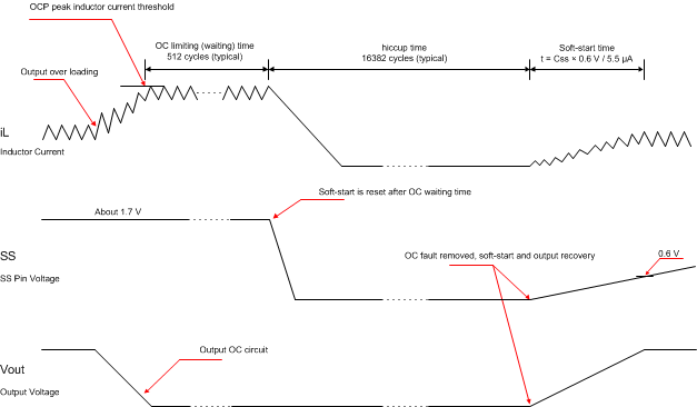 Figure 29. Overcurrent Protection
7.3.10 Power Good
The PGOOD pin is an open-drain output. After the feedback voltage of each buck is higher than 95% (rising) of the internal voltage reference, the PGOOD pin pulldown is deasserted and the pin floats. TI recommends to use a pullup resistor between the values of 10 kΩ and 100 kΩ to a voltage source that is 5.0 V or less.
The PGOOD pin is pulled low when any feedback voltage of a buck is lower than 92.5% (falling) of the nominal internal reference voltage. Also, the PGOOD is pulled low if the input voltage is undervoltage locked up, thermal shutdown is asserted, the EN pin is pulled low, or the converter is in a soft-start period.
7.3.11 Adjustable Switching Frequency
The ROSC pin can be used to set the switching frequency by connecting a resistor to GND. The switching frequency of the device is adjustable from 250 kHz to 2.4 MHz.
To determine the ROSC resistance for a given switching frequency, use Equation 6 or the curve in Figure 30. To reduce the solution size, the user should set the switching frequency as high as possible, but consider the tradeoffs of the supply efficiency and minimum controllable on-time.

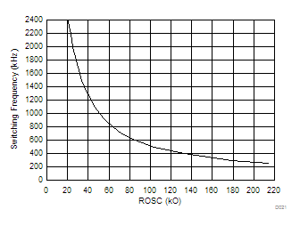 Figure 30. ROSC vs Switching Frequency
When an external clock applies to the ROSC pin, the internal phase locked loop (PLL) has been implemented to allow internal clock synchronizing to an external clock between 250 kHz and 2.4 MHz. To implement the clock synchronization feature, connect a square wave clock signal to the ROSC pin with a duty cycle between 20% to 80%. The clock signal amplitude must transition lower than 0.4 V and higher than 2.0 V. The start of the switching cycle is synchronized to the falling edge of the ROSC pin.
In applications where both resistor mode and synchronization mode are needed, the device can be configured as shown in Figure 31. Before an external clock is present, the device works in resistor mode and ROSC resistor sets the switching frequency. When an external clock is present, the synchronization mode overrides the resistor mode. The first time the ROSC pin is pulled above the ROSC high threshold (2.0 V), the device switches from the resistor mode to the synchronization mode and the ROSC pin becomes high impedance as the PLL starts to lock onto the frequency of the external clock. TI does not recommended to switch from synchronization mode back to resistor mode because the internal switching frequency drops to 100 kHz first before returning to the switching frequency set by ROSC resistor.
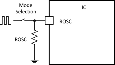 Figure 31. Works With Resistor Mode and Synchronization Mode
7.3.12 Thermal Shutdown
The internal thermal shutdown circuitry forces the device to stop switching if the junction temperature exceeds 160°C typically. The device reinitiates the power-up sequence when the junction temperature drops below 140°C typically.
7.4 Device Functional Modes
7.4.1 Operation With VIN < 2.6 V (Minimum VIN)
The device operates with input voltages above 2.6 V. The maximum UVLO voltage is 2.6 V and will operate at input voltages above 2.6 V. The typical UVLO voltage is 2.45 V and the device may operate at input voltages above that point. The device also may operate at lower input voltages, the minimum UVLO voltage is 2.35 V (rising) and 2.15V (falling). At input voltages below the UVLO minimum voltage, the devices will not operate.
7.4.2 Operation With EN Control
The enable rising edge threshold voltage is 1.2 V typical and 1.26 V maximum. With EN held below that voltage the device is disabled and switching is inhibited. The IC quiescent current is reduced in this state. When input voltage is above the UVLO threshold and the EN voltage is increased above the rising edge threshold, the device becomes active. Switching is enabled, and the soft start sequence is initiated. The device will start at the soft start time determined by the external soft start capacitor as shown in Figure 34 to Figure 36.