SLVSCT9B November 2014 – January 2015 TPS65266
PRODUCTION DATA.
- 1 Features
- 2 Applications
- 3 Description
- 4 Revision History
- 5 Pin Configuration and Functions
- 6 Specifications
-
7 Detailed Description
- 7.1 Overview
- 7.2 Functional Block Diagram
- 7.3
Feature Description
- 7.3.1 Adjusting the Output Voltage
- 7.3.2 Enable and Adjusting UVLO
- 7.3.3 Soft-Start Time
- 7.3.4 Power-Up Sequencing
- 7.3.5 Boostrap Voltage and BST-LX UVLO
- 7.3.6 Out of Phase Operation
- 7.3.7 Output Overvoltage Protection (OVP)
- 7.3.8 Slope Compensation
- 7.3.9 Overcurrent Protection
- 7.3.10 Power Good
- 7.3.11 Adjustable Switching Frequency
- 7.3.12 Thermal Shutdown
- 7.4 Device Functional Modes
- 8 Application and Implementation
- 9 Power Supply Recommendations
- 10Layout
- 11Device and Documentation Support
- 12Mechanical, Packaging, and Orderable Information
Package Options
Mechanical Data (Package|Pins)
- RHB|32
Thermal pad, mechanical data (Package|Pins)
- RHB|32
Orderable Information
10 Layout
10.1 Layout Guidelines
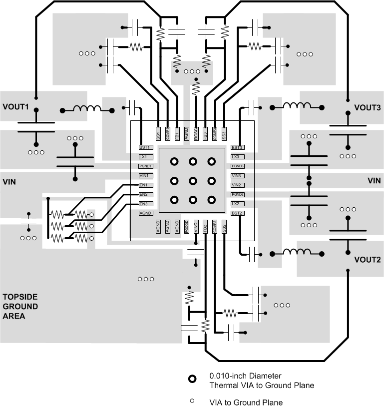
The TPS65266 supports a 2-layer PCB layout, shown in Figure 50.
Layout is a critical portion of good power supply design. See Figure 50 for a PCB layout example. The top contains the main power traces for VIN, VOUT, and LX. The top layer also has connections for the remaining pins of the TPS65266 and a large top-side area filled with ground. The top-layer ground area should be connected to the bottom layer ground using vias at the input bypass capacitor, the output filter capacitor, and directly under the TPS65266 device to provide a thermal path from the exposed thermal pad land to ground. The bottom layer acts as ground plane connecting analog ground and power ground.
For operation at full-rated load, the top-side ground area together with the bottom-side ground plane must provide an adequate heat dissipating area. Several signals paths conduct fast changing currents or voltages that can interact with stray inductance or parasitic capacitance to generate noise or degrade the power supplies' performance. To help eliminate these problems, the VIN pin should be bypassed to ground with a low-ESR ceramic bypass capacitor with X5R or X7R dielectric. Take care to minimize the loop area formed by the bypass capacitor connections, the VIN pins, and the ground connections. The VIN pin must also be bypassed to ground using a low-ESR ceramic capacitor with X5R or X7R dielectric.
Because the LX connection is the switching node, the output inductor should be located close to the LX pins, and the area of the PCB conductor minimized to prevent excessive capacitive coupling. The output filter capacitor ground should use the same power ground trace as the VIN input bypass capacitor. Try to minimize this conductor length while maintaining adequate width. The small signal components should be grounded to the analog ground path.
The FB and COMP pins are sensitive to noise so the resistors and capacitors should be located as close as possible to the IC and routed with minimal lengths of trace. Place the additional external components approximately as shown in Figure 50.
10.2 Layout Example
 Figure 50. PCB Layout