SLVSE48C january 2018 – may 2023 TPS65268-Q1
PRODUCTION DATA
- 1
- 1 Features
- 2 Applications
- 3 Description
- 4 Revision History
- 5 Pin Configuration and Functions
- 6 Specifications
-
7 Detailed Description
- 7.1 Overview
- 7.2 Functional Block Diagram
- 7.3
Feature Description
- 7.3.1 Adjusting the Output Voltage
- 7.3.2 Enable and Adjusting UVLO
- 7.3.3 Soft-Start Time
- 7.3.4 Power-Up Sequencing
- 7.3.5 V7V Low-Dropout Regulator and Bootstrap
- 7.3.6 Out-of-Phase Operation
- 7.3.7 Output Overvoltage Protection (OVP)
- 7.3.8 Slope Compensation
- 7.3.9 Overcurrent Protection
- 7.3.10 Power Good
- 7.3.11 Thermal Shutdown
- 7.4 Device Functional Modes
- 8 Application and Implementation
- 9 Device and Documentation Support
- 10Mechanical, Packaging, and Orderable Information
Package Options
Mechanical Data (Package|Pins)
- RHB|32
Thermal pad, mechanical data (Package|Pins)
- RHB|32
Orderable Information
3 Description
The TPS65268-Q1 device incorporates triple-synchronous buck converters with 4-V to 8-V wide input voltage. The converter with constant frequency peak current mode is designed to simplify its application while giving designers options to optimize the system according to targeted applications. The switching frequency of the converters is adjustable from 200 kHz to 2.3 MHz with an external resistor. Operation that is 180° out-of-phase between BUCK1 and BUCK2, and BUCK3 (BUCK2 and BUCK3 run in phase) minimizes the input filter requirements.
Each buck converter in the TPS65268-Q1 device operates in forced continuous-current mode (FCCM) at light load condition for reduced output voltage ripple and improved load transient response.
The TPS65268-Q1 device features overvoltage, overcurrent, short-circuit, and overtemperature protection.
| PART NUMBER | PACKAGE | BODY SIZE (NOM) |
|---|---|---|
| TPS65268-Q1 | RHB (VQFN, 32) | 5.00 mm × 5.00 mm |
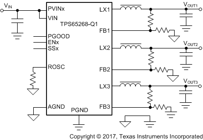
 Application Schematic
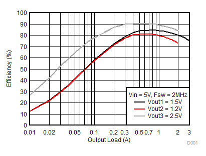
 Efficiency vs Output
Load