SLVSAX7E August 2011 – August 2016 TPS65270
PRODUCTION DATA.
- 1 Features
- 2 Applications
- 3 Description
- 4 Revision History
- 5 Description (continued)
- 6 Pin Configuration and Functions
- 7 Specifications
- 8 Detailed Description
- 9 Application and Implementation
- 10Power Supply Recommendations
- 11Layout
- 12Device and Documentation Support
- 13Mechanical, Packaging, and Orderable Information
Package Options
Mechanical Data (Package|Pins)
Thermal pad, mechanical data (Package|Pins)
Orderable Information
1 Features
- Wide Input Supply Voltage Range: 4.5 V to 18 V
- 0.8 V, ±1% Accuracy Reference
- Up to 2-A (Buck 1) and 3-A (Buck 2) Maximum Continuous Output Loading Current
- Low-Power Pulse Skipping Mode to Achieve High Light Load Efficiency
- Adjustable Switching Frequency
300 kHz to 1.4 MHz Set by External Resistor - Startup With a Prebiased Output Voltage
- Dedicated Enable and Soft Start for Each Buck
- Peak Current-Mode Control With Simple Compensation Circuit
- Cycle-by-Cycle Overcurrent Protection
- 180° Out-of-Phase Operation to Reduce Input Capacitance and Power Supply Induced Noise
- Available in 24-Lead Thermally Enhanced HTSSOP (PWP) and VQFN 4-mm × 4-mm (RGE) Packages
2 Applications
- DTV
- DSL Modems
- Cable Modems
- Set-Top Boxes
- Car DVD Players
- Home Gateway and Access Point Networks
- Wireless Routers
3 Description
The TPS65270 is a monolithic, dual synchronous buck regulator with a wide operating input voltage that can operate in 5-V, 9-V, 12-V, or 15-V bus voltages and battery chemistries. The converters are designed to simplify its application while giving the designer the option to optimize their usage according to the target application.
The TPS65270 features a precision 0.8-V reference and can produce output voltages up to 15 V. Each converter features an enable pin that allows dedicated control of each channel that provides flexibility for power sequencing. Soft-start time in each channel can be adjusted by choosing different external capacitors. TPS65270 is also able to start up with a prebiased output. The converter begins switching when output voltage reaches the prebiased voltage.
Constant frequency peak current-mode control simplifies the compensation and provides fast transient response. Cycle-by-cycle overcurrent protection and hiccup mode operation limits MOSFET power dissipation in short-circuit or overloading fault conditions. Low-side reverse current protection also prevents excessive sinking current from damaging the converter.
Device Information(1)
| PART NUMBER | PACKAGE | BODY SIZE (NOM) |
|---|---|---|
| TPS65270 | HTSSOP (24) | 7.80 mm × 4.40 mm |
| VQFN (24) | 4.00 mm × 4.00 mm |
- For all available packages, see the orderable addendum at the end of the data sheet.
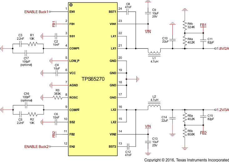
Typical Application

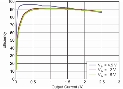
Efficiency vs Output Load
