SLVSCL3E June 2014 – May 2019 TPS65283 , TPS65283-1
PRODUCTION DATA.
- 1 Features
- 2 Applications
- 3 Description
- 4 Typical Schematic
- 5 Revision History
- 6 Description (continued)
- 7 Pin Configuration and Functions
- 8 Specifications
-
9 Detailed Description
- 9.1 Overview
- 9.2 Functional Block Diagram
- 9.3
Feature Description
- 9.3.1 Power Switch Detailed Description
- 9.3.2
Buck DC-DC Converter Detailed Description
- 9.3.2.1 Output Voltage
- 9.3.2.2 Adjustable Switching Frequency
- 9.3.2.3 Synchronization
- 9.3.2.4 Error Amplifier
- 9.3.2.5 Slope Compensation
- 9.3.2.6 Enable and Adjusting UVLO
- 9.3.2.7 Internal V7V Regulator
- 9.3.2.8 Short Circuit Protection
- 9.3.2.9 Bootstrap Voltage (BST) and Low Dropout Operation
- 9.3.2.10 Output Overvoltage Protection (OVP)
- 9.3.2.11 Power Good
- 9.3.2.12 Power-Up Sequencing
- 9.3.2.13 Thermal Performance
- 9.4 Device Functional Modes
- 10Application and Implementation
- 11Power Supply Recommendations
- 12Layout
- 13Device and Documentation Support
- 14Mechanical, Packaging, and Orderable Information
Package Options
Mechanical Data (Package|Pins)
- RGE|24
Thermal pad, mechanical data (Package|Pins)
- RGE|24
Orderable Information
10.2.2.7 Compensation Component Selection
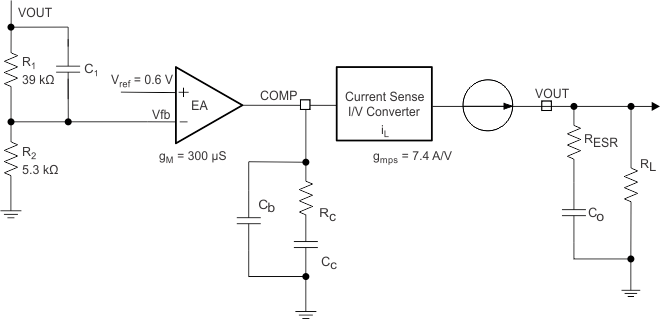
Integrated buck converters in TPS65283, TPS65283-1 incorporate a peak current mode. The error amplifier is a transconductance amplifier with a gain of 300 µA/V. A typical type II compensation circuit adequately delivers a phase margin between 60° and 90°. Cb adds a high-frequency pole to attenuate high-frequency noise when needed. To calculate the external compensation components, follow these steps.
- Select switching frequency ƒSW that is appropriate for application depending on L and C sizes, output ripple, EMI, and so forth. Switching frequency between 500 kHz to 1 MHz gives the best trade-off between performance and cost. To optimize efficiency, lower switching frequency is desired.
- Set up crossover frequency, ƒc, which is typically between 1/5 and 1/20 of ƒSW.
- RC can be determined by:
- gM is the error amplifier gain (300 µA/V),
- gmps is the power stage voltage to current conversion gain (7.4 A/V).
- Calculate CC by placing a compensation zero at or before the dominant pole (
 )
) - Optional Cb can be used to cancel the 0 from the ESR associated with Cb.
- Type III compensation can be implemented with the addition of one capacitor, C1. This allows for slightly higher loop bandwidths and higher phase margins. If used, C1 is calculated from Equation 20.
Equation 17. 

where
Equation 18. 

Equation 19. 

Equation 20. 

For this design, the calculated values for the compensation components are Rc = 20 kΩ, CC = 3.3 nF, and
Cb = 22 pF.
 Figure 31. DC-DC Loop Compensation