SLVSCL3E June 2014 – May 2019 TPS65283 , TPS65283-1
PRODUCTION DATA.
- 1 Features
- 2 Applications
- 3 Description
- 4 Typical Schematic
- 5 Revision History
- 6 Description (continued)
- 7 Pin Configuration and Functions
- 8 Specifications
-
9 Detailed Description
- 9.1 Overview
- 9.2 Functional Block Diagram
- 9.3
Feature Description
- 9.3.1 Power Switch Detailed Description
- 9.3.2
Buck DC-DC Converter Detailed Description
- 9.3.2.1 Output Voltage
- 9.3.2.2 Adjustable Switching Frequency
- 9.3.2.3 Synchronization
- 9.3.2.4 Error Amplifier
- 9.3.2.5 Slope Compensation
- 9.3.2.6 Enable and Adjusting UVLO
- 9.3.2.7 Internal V7V Regulator
- 9.3.2.8 Short Circuit Protection
- 9.3.2.9 Bootstrap Voltage (BST) and Low Dropout Operation
- 9.3.2.10 Output Overvoltage Protection (OVP)
- 9.3.2.11 Power Good
- 9.3.2.12 Power-Up Sequencing
- 9.3.2.13 Thermal Performance
- 9.4 Device Functional Modes
- 10Application and Implementation
- 11Power Supply Recommendations
- 12Layout
- 13Device and Documentation Support
- 14Mechanical, Packaging, and Orderable Information
Package Options
Mechanical Data (Package|Pins)
- RGE|24
Thermal pad, mechanical data (Package|Pins)
- RGE|24
Orderable Information
9.3.1.3 nFAULT Response
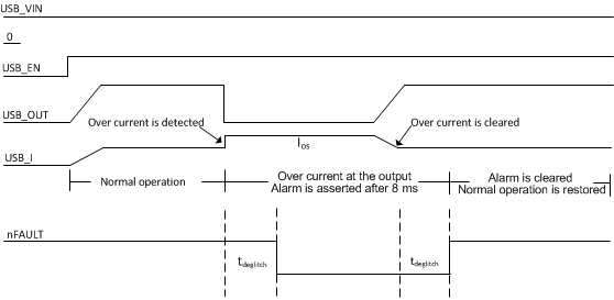
The nFAULT open‐drain output is asserted (active low) during an overcurrent, overtemperature, or reverse‐voltage condition. The TPS65283, TPS65283-1 asserts the nFAULT signal during a fault condition and remains asserted while the part is latched‐off. The nFAULT signal is deasserted when device power is cycled or the enable is toggled, and the device resumes normal operation. The TPS65283, TPS65283-1 is designed to eliminate false nFAULT reporting by using an internal delay "deglitch" circuit for over-current (8 ms typical) and reverse‐voltage (4 ms typical) conditions without the need for external circuitry. This ensures that nFAULT is not accidentally asserted due to normal operation such as starting into a heavy capacitive load. Deglitching circuitry delays entering and leaving fault conditions. Overtemperature conditions are not deglitched and assert the FAULT signal immediately.
 Figure 22. USB Switches Over Current