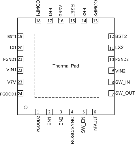
| PGOOD2 |
1 |
Power good indicator pin. Asserts low if the output voltage of buck2 is out of range due to thermal shutdown, dropout, over-voltage, EN, shutdown, or during slow start. |
| EN1 |
2 |
Enable pin for buck 1. A high signal on this pin enables buck1. For a delayed start-up, add a small ceramic capacitor from this pin to ground. |
| EN2 |
3 |
Enable pin for buck 2. A high signal on this pin enables buck2. For a delayed start-up, add a small ceramic capacitor from this pin to ground. |
| ROSC/SYNC |
4 |
Automatically select clock frequency program mode and clock synchronization mode. Program the switching frequency of the device from 200 kHz to 2 MHz with an external resistor connecting to the pin. In clock synchronization mode, the device automatically synchronizes to an external clock applied to the pin. |
| SW_EN |
5 |
Enable power switch. Float to enable. |
| nFAULT |
6 |
Active low open-drain output. Asserted during overcurrent or reverse-voltage condition of power switch. |
| SW_OUT |
7 |
Power switch output |
| SW_IN |
8 |
Power switch input |
| VIN2 |
9 |
Input power supply for buck2. Connect this pin as close as possible to the (+) terminal of input ceramic capacitor (10 µF suggested). |
| PGND2 |
10 |
Power ground connection. Connect this pin as close as possible to the (–) terminal of input capacitor of buck2. |
| LX2 |
11 |
Switching node connection to the inductor and bootstrap capacitor for buck2 converter. This pin voltage swings from a diode voltage below the ground up to input voltage of buck2. |
| BST2 |
12 |
Bootstrapped supply to the high-side floating gate driver in buck converter. Connect a capacitor (47 nF recommended) from this pin to LX2. |
| COMP2 |
13 |
Error amplifier output and loop compensation pin for buck2. Connect a series resistor and capacitor to compensate the control loop of buck2 with peak current PWM mode. |
| FB2 |
14 |
Feedback sensing pin for buck2 output voltage. Connect this pin to the resistor divider of buck2 output. The feedback reference voltage is 0.6 V ±1%. |
| RSET |
15 |
Power switch current limit control pin. An external resistor used to set current limit threshold of power switch. Recommended 9.1 kΩ ≤ RSET ≤ 80.6 kΩ. |
| AGND |
16 |
Analog ground common to buck controller and power switch controller. AGND must be routed separately from high current power grounds to the (–) terminal of bypass capacitor of internal V7V LDO output. |
| FB1 |
17 |
Feedback sensing pin for buck1 output voltage. Connect this pin to the resistor divider of buck1 output. The feedback reference voltage is 0.6 V ±1%. |
| COMP1 |
18 |
Error amplifier output and loop compensation pin for buck1. Connect a series resistor and capacitor to compensate the control loop of buck1 converter with peak current PWM mode. |
| BST1 |
19 |
Bootstrapped supply to the high side floating gate driver in buck converter. Connect a capacitor (recommend 47 nF) from this pin to LX1. |
| LX1 |
20 |
Switching node connection to the inductor and bootstrap capacitor for buck1. This pin voltage swings from a diode voltage below the ground up to input voltage of buck1. |
| PGND1 |
21 |
Power ground connection. Connect this pin as close as possible to the (–) terminal of input capacitor of buck1. |
| VIN1 |
22 |
Input power supply for buck1 and internal analog bias circuitries. Connect this pin as close as possible to the (+) terminal of an input ceramic capacitor (10 µF suggested). |
| V7V |
23 |
Internal linear regulator (LDO) output with input from VIN1. The internal driver and control circuits are powered from this voltage. Decouple this pin to power ground with a minimum 1-µF ceramic capacitor. The output voltage level of LDO is regulated to typical 6.3 V for optimal conduction on-resistances of internal power MOSFETs. In PCB design, the power ground and analog ground should have one-point common connection at the (–) terminal of V7V bypass capacitor. |
| PGOOD1 |
24 |
Power good indicator pin. Asserts low if the output voltage of buck1 is out of range due to thermal shutdown, dropout, over-voltage, EN shutdown or during slow start. |
| PowerPAD™ |
— |
Exposed pad beneath the IC. Connect to the power ground. Always solder power pad to the board, and have as many vias as possible on the PCB to enhance power dissipation. There is no electric signal down bonded to paddle inside the IC package. |
