SLVSBB6F March   2012  – July 2015 TPS65300-Q1

PRODUCTION DATA.  

  1. Features
  2. Applications
  3. Description
  4. Revision History
  5. Pin Configuration and Functions
  6. Specifications
    1. 6.1  Absolute Maximum Ratings
    2. 6.2  ESD Ratings
    3. 6.3  Recommended Operating Conditions
    4. 6.4  Thermal Information
    5. 6.5  DC Characteristics
    6. 6.6  Timing Requirements
    7. 6.7  Switching Characteristics
    8. 6.8  Typical Characteristics
    9. 6.9  5-V Linear Regulator (5VO)
    10. 6.10 3.3-V Linear Regulator Controller (3.3VO)
    11. 6.11 1.234-V Linear Regulator Controller (1.2VO)
  7. Detailed Description
    1. 7.1 Overview
    2. 7.2 Functional Block Diagram
    3. 7.3 Feature Description
      1. 7.3.1 Detailed Pin Descriptions
      2. 7.3.2 Buck Converter
        1. 7.3.2.1  PWM Operation
        2. 7.3.2.2  Voltage-Mode Control Loop
        3. 7.3.2.3  Output Voltage 5.3 V (VREG)
        4. 7.3.2.4  Switching Frequency (RT/CLK)
        5. 7.3.2.5  Boost Capacitor (BOOT)
        6. 7.3.2.6  Soft Start (SS)
        7. 7.3.2.7  Power-On Delay (DELAY)
        8. 7.3.2.8  Reset (nRST)
        9. 7.3.2.9  Thermal Shutdown
        10. 7.3.2.10 Reset Function
      3. 7.3.3 Linear Regulators
        1. 7.3.3.1 Fixed Linear Regulator Output (5.3 V)
        2. 7.3.3.2 Fixed Linear Regulator Controller (3.3 V)
        3. 7.3.3.3 Fixed Linear Regulator Controller (1.2 V)
    4. 7.4 Device Functional Modes
      1. 7.4.1 Operational Mode
      2. 7.4.2 Buck Converter Modes of Operation
        1. 7.4.2.1 Continuous-Conduction Mode (CCM)
        2. 7.4.2.2 Discontinuous Mode (DCM)
        3. 7.4.2.3 Tracking Mode
  8. Application and Implementation
    1. 8.1 Application Information
    2. 8.2 Typical Application
      1. 8.2.1 Design Requirements
      2. 8.2.2 Detailed Design Procedure
        1. 8.2.2.1 Duty Cycle
        2. 8.2.2.2 Output Inductor Selection (L)
        3. 8.2.2.3 Output Capacitor Selection (CO)
        4. 8.2.2.4 External Schottky Diode (D)
        5. 8.2.2.5 Input Capacitor (CI)
        6. 8.2.2.6 Loop Compensation
        7. 8.2.2.7 Loop-Control Frequency Compensation
          1. 8.2.2.7.1 Type III Compensation
          2. 8.2.2.7.2 PWM Modulator Gain K
          3. 8.2.2.7.3 Resistor Values
          4. 8.2.2.7.4 Gain of Amplifier
          5. 8.2.2.7.5 Poles and Zero Frequencies
        8. 8.2.2.8 Power Dissipation
          1. 8.2.2.8.1 Switch-Mode Power-Supply Losses
      3. 8.2.3 Application Curves
  9. Power Supply Recommendations
  10. 10Layout
    1. 10.1 Layout Guidelines
      1. 10.1.1 Inductor L
      2. 10.1.2 Input Filter Capacitors CI
      3. 10.1.3 Feedback
      4. 10.1.4 Traces and Ground Plane
    2. 10.2 Layout Example
  11. 11Device and Documentation Support
    1. 11.1 Device Support
      1. 11.1.1 Third-Party Products Disclaimer
    2. 11.2 Documentation Support
      1. 11.2.1 Related Documentation
    3. 11.3 Community Resource
    4. 11.4 Trademarks
    5. 11.5 Electrostatic Discharge Caution
    6. 11.6 Glossary
  12. 12Mechanical, Packaging, and Orderable Information

Package Options

Mechanical Data (Package|Pins)
Thermal pad, mechanical data (Package|Pins)
Orderable Information

5 Pin Configuration and Functions

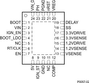
RHF Package
24-Pin VQFN With Exposed Thermal Pad
Top View
TPS65300-Q1 P0057-02_SLVSBB6.gif
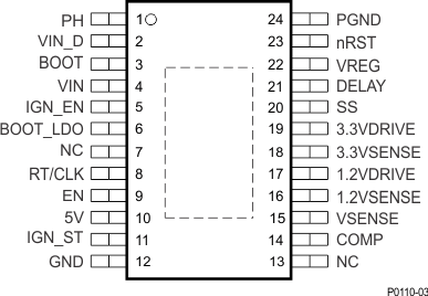
PWP Package
24-Pin HTSSOP With PowerPAD™
Top View
TPS65300-Q1 P0110-03_SLVSBB6.gif

Pin Functions

PIN I/O DESCRIPTION
NAME NO.
PWP RHF
1.2VDRIVE 17 15 O Output current source to drive the base of an external bipolar transistor to regulate the 1.234-V supply
1.2VSENSE 16 14 I Voltage node of 1.234-V supply
3.3VDRIVE 19 17 O Output current source to drive the base of an external bipolar transistor to regulate the 3.3-V supply
3.3VSENSE 18 16 I Voltage node of 3.3-V supply
5V 10 8 O External capacitor to ground for stability of regulated output
BOOT 3 1 O External bootstrap capacitor connected to PH (pin 1) to drive gate of internal switching FET
BOOT_LDO 6 4 O External capacitor connected to ground for stability of internal regulator
COMP 14 12 O Error amplifier output to connect external compensation components
DELAY 21 19 O External capacitor to ground to program the power-on-reset delay
EN 9 7 I A high logic-level input signal to enable and low signal to disable device. Internally pulled down to ground
GND 12 10 O Ground pin, must be electrically connected to exposed pad on PCB for proper thermal performance
IGN_EN 5 3 I Ignition input (high-voltage tolerant) internally pulls to ground. Must be externally pulled up to enable
IGN_ST 11 9 O Active-low, open-drain ignition input indicator, output connected to external bias voltage through a resistor. Asserted high after ignition input is high
NC 7 5 Connect to ground
13 11
nRST 23 21 O Active-low, open-drain reset output connected to external bias voltage through a resistor. This output is asserted high after the preregulator, 3.3-V, and 1.234-V regulator outputs are regulating and the delay timer has expired. Also, output is asserted low if any one of these three supplies is out of the set regulation, this threshold is internally set.
PGND 24 22 O Power ground pin, must be electrically connected to exposed pad on PCB for proper thermal performance
PH 1 23 O Source of internal switching FET
RT/CLK 8 6 I/O External resistor connected ground to program the internal oscillator. Alternative option is to feed an external clock to provide reference for switching frequency.
SS 20 18 O External capacitor to ground to program soft-start time
VIN 4 2 I Unregulated input voltage supply. Pins 2 and 4 must be connected together externally.
VIN_D 2 24 I Drain input for internal high-side MOSFET. Pins 2 and 4 must be connected together externally.
VREG 22 20 I Buck converter output. Integrated internal low-side FET to load output during startup or limit voltage overshoot
VSENSE 15 13 I Inverting node of error amplifier for voltage-mode control of preregulated supply
Thermal pad Electrically connect to ground and solder to ground plane of PCB for thermal efficiency