SLVSBB6F March   2012  – July 2015 TPS65300-Q1

PRODUCTION DATA.  

  1. Features
  2. Applications
  3. Description
  4. Revision History
  5. Pin Configuration and Functions
  6. Specifications
    1. 6.1  Absolute Maximum Ratings
    2. 6.2  ESD Ratings
    3. 6.3  Recommended Operating Conditions
    4. 6.4  Thermal Information
    5. 6.5  DC Characteristics
    6. 6.6  Timing Requirements
    7. 6.7  Switching Characteristics
    8. 6.8  Typical Characteristics
    9. 6.9  5-V Linear Regulator (5VO)
    10. 6.10 3.3-V Linear Regulator Controller (3.3VO)
    11. 6.11 1.234-V Linear Regulator Controller (1.2VO)
  7. Detailed Description
    1. 7.1 Overview
    2. 7.2 Functional Block Diagram
    3. 7.3 Feature Description
      1. 7.3.1 Detailed Pin Descriptions
      2. 7.3.2 Buck Converter
        1. 7.3.2.1  PWM Operation
        2. 7.3.2.2  Voltage-Mode Control Loop
        3. 7.3.2.3  Output Voltage 5.3 V (VREG)
        4. 7.3.2.4  Switching Frequency (RT/CLK)
        5. 7.3.2.5  Boost Capacitor (BOOT)
        6. 7.3.2.6  Soft Start (SS)
        7. 7.3.2.7  Power-On Delay (DELAY)
        8. 7.3.2.8  Reset (nRST)
        9. 7.3.2.9  Thermal Shutdown
        10. 7.3.2.10 Reset Function
      3. 7.3.3 Linear Regulators
        1. 7.3.3.1 Fixed Linear Regulator Output (5.3 V)
        2. 7.3.3.2 Fixed Linear Regulator Controller (3.3 V)
        3. 7.3.3.3 Fixed Linear Regulator Controller (1.2 V)
    4. 7.4 Device Functional Modes
      1. 7.4.1 Operational Mode
      2. 7.4.2 Buck Converter Modes of Operation
        1. 7.4.2.1 Continuous-Conduction Mode (CCM)
        2. 7.4.2.2 Discontinuous Mode (DCM)
        3. 7.4.2.3 Tracking Mode
  8. Application and Implementation
    1. 8.1 Application Information
    2. 8.2 Typical Application
      1. 8.2.1 Design Requirements
      2. 8.2.2 Detailed Design Procedure
        1. 8.2.2.1 Duty Cycle
        2. 8.2.2.2 Output Inductor Selection (L)
        3. 8.2.2.3 Output Capacitor Selection (CO)
        4. 8.2.2.4 External Schottky Diode (D)
        5. 8.2.2.5 Input Capacitor (CI)
        6. 8.2.2.6 Loop Compensation
        7. 8.2.2.7 Loop-Control Frequency Compensation
          1. 8.2.2.7.1 Type III Compensation
          2. 8.2.2.7.2 PWM Modulator Gain K
          3. 8.2.2.7.3 Resistor Values
          4. 8.2.2.7.4 Gain of Amplifier
          5. 8.2.2.7.5 Poles and Zero Frequencies
        8. 8.2.2.8 Power Dissipation
          1. 8.2.2.8.1 Switch-Mode Power-Supply Losses
      3. 8.2.3 Application Curves
  9. Power Supply Recommendations
  10. 10Layout
    1. 10.1 Layout Guidelines
      1. 10.1.1 Inductor L
      2. 10.1.2 Input Filter Capacitors CI
      3. 10.1.3 Feedback
      4. 10.1.4 Traces and Ground Plane
    2. 10.2 Layout Example
  11. 11Device and Documentation Support
    1. 11.1 Device Support
      1. 11.1.1 Third-Party Products Disclaimer
    2. 11.2 Documentation Support
      1. 11.2.1 Related Documentation
    3. 11.3 Community Resource
    4. 11.4 Trademarks
    5. 11.5 Electrostatic Discharge Caution
    6. 11.6 Glossary
  12. 12Mechanical, Packaging, and Orderable Information

Package Options

Mechanical Data (Package|Pins)
Thermal pad, mechanical data (Package|Pins)
Orderable Information

6 Specifications

6.1 Absolute Maximum Ratings

over operating free-air temperature range (unless otherwise noted)(1)
MIN MAX UNIT
Buck regulator VIN, VIN_D –0.3 45 V
BOOT –0.3 50 V
PH –1
–2 for 30 ns
45 V
VSENSE –0.3 5.5 V
Control IGN_EN –0.3 45 V
EN, 3.3VSENSE, 1.2VSENSE, RT/CLK, VREG –0.3 5.5 V
Output 3.3VDRIVE, 1.2VDRIVE –0.3 8 V
nRST, IGN_ST –0.3 5.5 V
DELAY, COMP –0.3 7 V
BOOT_LDO, 5V –0.3 9 V
Operating junction temperature, TJ –40 150 °C
Storage temperature, TstgMoved the storage temperature and ESD ratings out of the Absolute Maximum Ratings table and into the new Handling Ratings table –55 165 °C
(1) Stresses beyond those listed under Absolute Maximum Ratings may cause permanent damage to the device. These are stress ratings only, and functional operation of the device at these or any other conditions beyond those indicated under Recommended Operating Conditions is not implied. Exposure to absolute-maximum-rated conditions for extended periods may affect device reliability.

6.2 ESD Ratings

VALUE UNIT
V(ESD) Electrostatic discharge Human-body model (HBM), per AEC Q100-002(1) ±2000 V
Charged-device model (CDM), per AEC Q100-011 All pins ±500
Corner pins (1, 12, 13, and 24) ±750
(1) AEC Q100-002 indicates that HBM stressing shall be in accordance with the ANSI/ESDA/JEDEC JS-001 specification.

6.3 Recommended Operating Conditions

over operating free-air temperature range (unless otherwise noted)
MIN NOM MAX UNIT
VIN, VIN_D 5.6 40 V
BOOT 5.6 48 V
PH –1 40 V
IGN_EN 0 40 V
EN, VSENSE, 3.3VSENSE, 1.2VSENSE, RT/CLK, nRST, IGN_ST 0 5.25 V
VREG, 3.3VDRIVE, 1.2VDRIVE 0 7.5 V
SS, DELAY, COMP 0 6.5 V
BOOT_LDO 0 8.1 V
Operating ambient temperature range, TA –40 125 °C

6.4 Thermal Information

THERMAL METRIC(1) TPS65300-Q1 UNIT
PWP (HTSSOP) RHF (VQFN)
24 PINS 24 PINS
RθJA Junction-to-ambient thermal resistance 33.6 30.3 °C/W
RθJC(top) Junction-to-case (top) thermal resistance 16.6 30.5 °C/W
RθJB Junction-to-board thermal resistance 14.5 8.7 °C/W
ψJT Junction-to-top characterization parameter 0.4 0.3 °C/W
ψJB Junction-to-board characterization parameter 14.3 8.8 °C/W
RθJC(bot) Junction-to-case (bottom) thermal resistance 1.3 1.6 °C/W
(1) For more information about traditional and new thermal metrics, see the Semiconductor and IC Package Thermal Metrics application report, SPRA953.

6.5 DC Characteristics

VIN = 6 V to 27 V, IGN_EN = VIN, TJ-Max = 150°C, unless otherwise noted
PARAMETER TEST CONDITIONS MIN TYP MAX UNIT
VIN, VIN_D (Input Power Supply)
VIN, VIN_D Supply voltage on VIN, line Normal mode, after initial start-up 5.6 14 40 V
Iq-Normal Current normal mode Open-loop test 4.57 mA
ISD VIN Shut down IGN = 0 V, VIN = 12 V, TA = -40°C to 125°C 2.2 15 µA
ISD VIND IGN = 0 V, VIN = 12 V, TA = -40°C to 125°C 2.2 15
IGN_EN (Ignition Input)
VIGN_EN Input voltage range Input into IGN_EN pin 14 40 V
VIH Input high Enable device to be ON (rising signal) 3.16 3.6 V
VIL Input low Enable device to be OFF (falling signal) 2.2 3.03 V
IIH Input high Enable device to be ON,
VIGN_EN = 18 V
23.7 50 µA
Enable device to be ON,
VIGN_EN = 3.7 V
4 7
EN (Logic Level Enable)
VIH Input high Enable device to be ON (rising signal) 1.7 2.3 V
VIL Input low Enable device to be OFF (falling signal) 0.7 1.53 V
Switch-Mode Output 5.3 V
VREG Regulator output internal resistor network Fixed output based on internal resistor network 5.178 5.3 5.542 V
CO Output capacitor for 5.3 V ESR = 0.001 Ω to 100 mΩ; large output capacitance may be required for load transients 10 µF
rds(on) Internal switch resistance Measured across VIN_D and PH pins, IVREG = 1 A 0.3 Ω
IO-CL Switch current-limit VIN = 12 V 1.2 2 3 A
VSENSE (Internal Reference Voltage)
VREG ref Internal reference voltage 1.954 2 2.046 V
SS (Soft-Start Timer for Switch-Mode Converter)
ISS Soft-start source current Css = 0.001 µF to 0.01 µF 40 50 60 µA
IGN_ST (Ignition Input Status)
VOL Output low Output asserted low when IGN_EN < 2.2 V, IOL = 1 mA 0.056 0.4 V
IIH Leakage test IGN_ST = 5 V 0.05 2 µA
5V (5-V Linear Regulator)
5Vo Output voltage IO = 1 mA, VREG = 5.3 V 4.9 5 5.1 V
∆VO-Line Line regulation 5.15 V < VREG < 5.45 V, IO = 1 mA, VIN = 12 V 10 20 mV
∆VO-Load Load regulation 1 mA < IO < 200 mA, VREG = 5.3 V, VIN = 12 V 10 30 mV
VDO Dropout voltage IO = 150 mA, measure VREG when VO(nom) – 0.1 V, then VDO = VREG – (5VO – 0.1) V, VREG > 5 V 0.15 0.26 V
I5V-CL Current-limit 5VO = 0.8 × 5VO (nominal) 350 1080 mA
CO Output capacitor ESR = 0.001 Ω to 2 Ω. Larger output capacitance may be required for load transients. 1 2.2 10 µF
PSRR Power-supply rejection ratio f = 100 Hz, VREG = 5.3 V, IO = 100 mA, VIN = 12 V 45 60 75 dB
3.3-V Linear Regulator Controller (3.3VSENSE)
3.3VO Output voltage Io = 5 mA, Vnpn_power input = 5.3 V 3.234 3.3 3.366 V
∆3.3VO-Line Line regulation 3.8 V < Vnpn_power input < 7 V (with nRST not triggered) 1 10 mV
∆3.3VO-Load Load regulation 5 mA < IO < 550 mA 7.5 30 mV
CO Output capacitor for 3.3 V ESR = 0.001 Ω to 2 Ω. Large output capacitance may be required for load transients. 1 4.7 10 µF
PSRR Power-supply rejection ratio f = 100 Hz, VREG = 5.3 V, IO = 200 mA, VIN = 12 V 45 60 75 dB
3.3VDRIVE (Ex. Switch Control Output)
IOH Base drive current. NPN turn ON 3.3VDRIVE – 3.3VSENSE = 1 V 10 28 50 mA
IOL NPN turn off 3.3VDRIVE – 3.3VSENSE at 0.2V 0.1 0.412 mA
1.2-V Linear Regulator Controller (1.2VSENSE)
1.2VO Output voltage Io = 5 mA, Vnpn_power input = 5.3 V 1.209 1.234 1.259 V
∆1.2VO-Line Line regulation 3.25 V < Vnpn_power input < 7 V (with nRST not triggered) 1 10 mV
∆1.2VO-Load Load regulation 5 mA < IO < 350 mA 5 15 mV
CO Output capacitor for 1.2 V ESR = 0.001 Ω to 100 mΩ. Large output capacitance may be required for load transients. 8 10 12 µF
PSRR Power-supply rejection ratio f = 100 Hz, VREG = 6 V, IO = 200 mA, VIN = 12 V 45 60 75 dB
1.2VDRIVE (Ex. Switch Control Output)
IOH Base drive current. NPN turn ON 1.2VDRIVE – 1.2VSENSE = 1 V 10 27 50 mA
IOL NPN turn off 1.2VDRIVE – 1.2VSENSE at 0.2 V 0.1 0.47 mA
DELAY (Power-On-Reset Delay)
VThreshold Threshold voltage Threshold to release nRST high 1.3 2.05 2.6 V
ICharge Capacitor charging current 1.4 2 2.6 µA
nRST (Reset Indicator)
VOL Output low Reset asserted due to falling VREG or 3.3VO or 1.2VO output voltages, IOL = 1 mA 0 0.16 0.4 V
VTH_VREG Trigger nRST for VREG output VREG ramp down 0.87 0.9 0.93 VREG
Trigger nRST for 3.3VO 0.9 0.93 0.96 3.3 VO
Trigger nRST for 1.2VO 0.9 0.93 0.96 1.2 VO
IIH Leakage test Reset = 5 V 0.07 2 µA
RT/CLK (Oscillator Setting of External Clock Input)
VIH Input high 2.3 V
VIL Input low 0.6 V

6.6 Timing Requirements

MIN NOM MAX UNIT
Switch-Mode Output 5.3 V
tON-min Minimum ON time 40 ns
Dmax Maximum duty cycle 97%

6.7 Switching Characteristics

VIN = 6 V to 27 V, IGN_EN = VIN, TJ-Max = 150°C, unless otherwise noted
PARAMETER TEST CONDITIONS MIN TYP MAX UNIT
5V (5-V Linear Regulator)
Vsoft-start Soft start on enable cycle 5VO = 0 V (initially) with fsw = 2.5 MHz 13 ms
3.3-V Linear Regulator Controller (3.3VSENSE)
tss Soft-start time 3.3VO = 0 V (initially) with fsw = 2.5 MHz 12.3 ms
1.2-V Linear Regulator Controller (1.2VSENSE)
tss Soft-start time 1.2VO = 0 V (initially) with fsw= 2.5 MHz 8.5 ms
nRST (Reset Indicator)
tnRSTdly Filter time Delay before nRST is asserted low 11 µs
RT/CLK (Oscillator Setting of External Clock Input)
fsw Switching freq using RT mode 2 3 MHz
Switching freq using CLK mode 2 3 MHz
Minimum clock input pulse duration 40 ns
Internal oscillator frequency Switching frequency tolerance for clock –14% 14%
External clock input Switching frequency tolerance for clock –20% 10%

6.8 Typical Characteristics

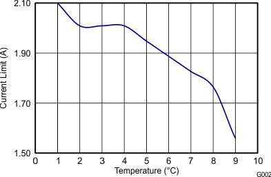
TPS65300-Q1 G002_SLVSBB6.gif
Figure 1. Buck Current-Limit vs Temperature
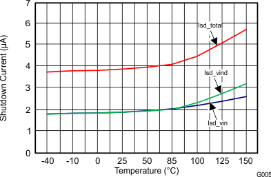
TPS65300-Q1 G005_SLVSBB6.gif
Figure 3. Current Consumption IIN vs Temperature
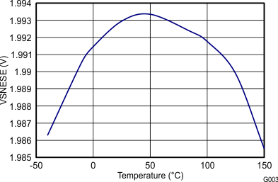
TPS65300-Q1 G003_SLVSBB6.gif
Figure 2. VSENSE Reference Voltage vs Temperature
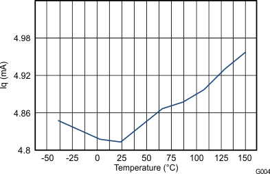
TPS65300-Q1 G004_SLVSBB6.gif
Figure 4. Quiescent Current vs Temperature

6.9 5-V Linear Regulator (5VO)

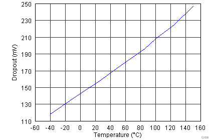
TPS65300-Q1 G006_SLVSBB6.png
Figure 5. Dropout Voltage vs Temperature
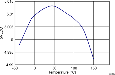
TPS65300-Q1 G007_SLVSBB6.gif
Figure 6. Output Voltage 5VO vs Temperature

6.10 3.3-V Linear Regulator Controller (3.3VO)
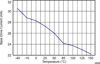
TPS65300-Q1 G008_SLVSBB6.gif
Figure 7. Output Base Drive vs Temperature
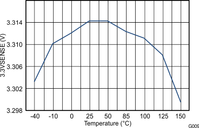
TPS65300-Q1 G009_SLVSBB6.gif
Figure 8. 3.3VSENSE vs Temperature

6.11 1.234-V Linear Regulator Controller (1.2VO)

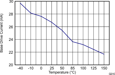
TPS65300-Q1 G010_SLVSBB6.gif
Figure 9. Output Base Drive vs Temperature
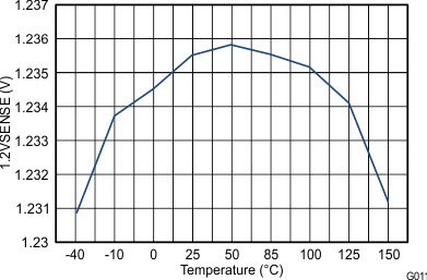
TPS65300-Q1 G011_SLVSBB6.gif
Figure 10. 1.2VSENSE vs Temperature