SLVSC10C October 2013 – April 2016 TPS65301-Q1
PRODUCTION DATA.
- 1 Features
- 2 Applications
- 3 Description
- 4 Revision History
- 5 Pin Configuration and Functions
- 6 Specifications
- 7 Detailed Description
-
8 Application and Implementation
- 8.1 Application Information
- 8.2
Typical Application
- 8.2.1 Design Requirements
- 8.2.2 Detailed Design Procedure
- 8.2.3 Application Curves
- 9 Power Supply Recommendations
- 10Layout
- 11Device and Documentation Support
- 12Mechanical, Packaging, and Orderable Information
Package Options
Mechanical Data (Package|Pins)
- PWP|24
Thermal pad, mechanical data (Package|Pins)
- PWP|24
Orderable Information
7 Detailed Description
7.1 Overview
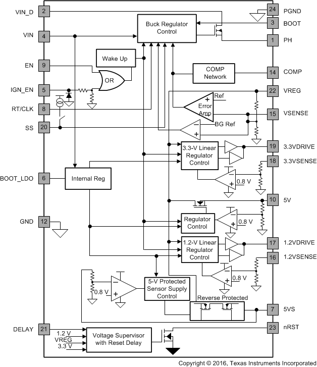
The device integrates an asynchronous switch-mode power-supply converter with a internal FET that converts the input battery voltage to a 5.45-V preregulator output. This 5.45-V output supplies the other regulators. The switching frequency range is from 2 MHz to 3 MHz, allowing the use of low-profile inductors and low value input and output capacitors. External loop compensation provides flexibility which optimizes the converter response for the appropriate operating condition.
A fixed 5-V linear regulator with an internal FET is integrated as an external peripheral supply. A fixed 3.3-V linear regulator controller with external bi-polar transistor is used for an IO supply, for example. A fixed 1.2-V linear regulator controller with external bi-polar transistor is used for a CPU Core supply, for example. The device has a voltage supervisor which monitors the output of the switch-mode power supply, the 3.3-V linear regulator, and the 1.2-V linear regulator.
An external timing capacitor sets the power-on delay and the release of the reset output nRST. This reset output is also used to indicate if the switch-mode supply, the 3.3-V linear regulator supply, or the 1.2-V linear regulator supply is outside the set limits. The 5-V regulator tracks the 3.3-V linear regulator within the specified limits.
7.2 Functional Block Diagram

7.3 Feature Description
7.3.1 Buck Converter
7.3.1.1 PWM Operation
The switch-mode power supply (SMPS) operates in a fixed-frequency pulse-width modulation (PWM) mode. The switching frequency is set by an external resistor or synchronized with an external clock input. The internal N-channel MOSFET is turned on at the beginning of each cycle. This MOSFET is turned off when the PWM comparator resets the latch. Once the high external FET is turned off, the external Schottky diode recirculates the energy stored in the inductor for the remainder of the switching period.
The external bootstrap capacitor acts as a voltage supply for the internal high-side MOSFET. This capacitor is recharged on every recirculation cycle (when the internal high-side MOSFET is turned OFF). In case of a VIN close to the desired output voltage, requiring a nearly 100% duty cycle for the internal high side MOSFET, the device automatically revert to 87% to allow the bootstrap capacitor to recharge.
7.3.1.2 Voltage-Mode Control Loop
The voltage-mode control monitors the set output voltage and processes the signal to control the internal MOSFET. A voltage feedback signal is compared to a constant ramp waveform, resulting in a PWM modulation pulse. An input line-voltage feedforward technique is incorporated to compensate for changes in the input voltage and ensures the output voltage is stable by adjusting the ramp waveform for the correct duty cycle. The internal MOSFET is protected from excess power dissipation with a current limit and frequency foldback circuitry during an output-to-ground short-circuit event.
A combination of internal and external components forms a compensation network to ensure error-amplifier gain does not cause instability due to input voltage changes or load perturbations.
7.3.1.3 Output Voltage 5.45 V (VREG)
Output voltage VREG is generated by the converter supplied from the battery voltage VIN and the external components (L, C). The output is sensed through an internal resistor divider and compared with an internal reference voltage.
This output requires larger output capacitors (4.7-µF to 10-µF range) to ensure that during load transients the output does not drop below the reset threshold for a period longer than the reset deglitch filter time.
An internal load is enabled for a short period whenever
- a start-up condition occurs, that is, during power up or when IGN_EN or EN is toggled.
- an overvoltage condition exists on this output.
7.3.1.4 Switching Frequency (RT/CLK)
The oscillator frequency of the buck regulator is selectable by means of a resistor placed at the RT/CLK pin to ground. The switching frequency (fSW) can be set in the range 2 MHz to 3 MHz in this resistor mode. Alternatively, if there is an external clock input signal, the internal oscillator synchronizes to this signal within 10 µs.
The following equation determines the value of resistor (RT) for the required switching frequency fSW.

7.3.1.5 Boost Capacitor (BOOT)
This capacitor provides the gate-drive voltage for the internal MOSFET switch. X7R and X5R grade dielectrics are recommended due to their stable values over temperature. Usually, a 0.1-µF capacitor is used for the boot capacitor.
7.3.1.6 Soft Start (SS)
To limit the start-up inrush current for the switch-mode supply, an internal soft-start circuit is used to ramp up the reference voltage from 0 V to the final value of 0.8 V. The regulator uses the internal reference or the SS-pin voltage as the power-supply reference voltage to regulate the output accordingly. The following equation determines the soft-start timing.

where
- C = Capacitor on SS pin, usually 0.1 µF or lower
7.3.1.7 Power-On Delay (DELAY)
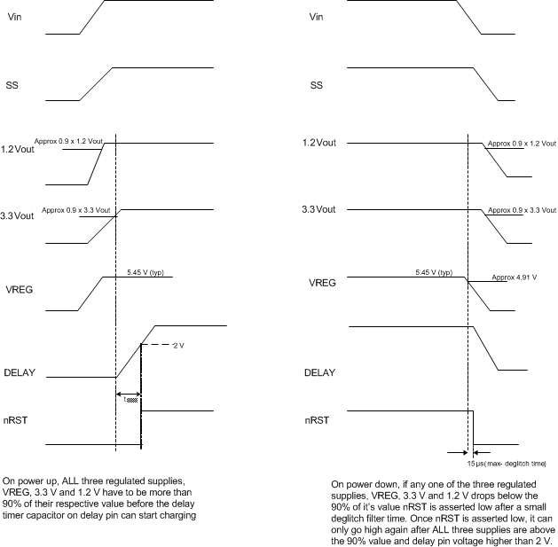
The power-on delay function delays the release of the nRST line. The method of operation is to detect when all VREG (5.45 V), 3.3-V and 1.2-V power-supply outputs are above 90% (typical) of the set value. This then triggers a current source to charge the external capacitor on the DELAY pin. Once this capacitor is charged to approximately 2 V, the nRST line is asserted high. The delay time is calculated using the following equation:

where
- C = capacitor on DELAY pin
Example: For a 20-ms delay, C = 20 nf.
7.3.1.8 Reset (nRST)
The nRST pin is an open-drain output. The power-on reset signal is a voltage supervisor output to indicate the output voltages on VREG (5.45 V), 3.3 V, and 1.2 V are within the specified tolerance of their set regulated voltages. Additionally, whenever both the IGN_EN and EN pins are low or open, nRST is immediately asserted low regardless of the output voltage. If a thermal shutdown occurs due to excessive thermal conditions, this pin is asserted low.
Conversely on power down, once the VREG or 3.3V or 1.2V output voltage falls below 90% of its respective set threshold, nRST is pulled low after a de-glitch filter delay of approximately 15 µs (max). This is implemented to prevent nRST from being invoked due to noise on the output supplies.
7.3.1.9 Thermal Shutdown
This device has two independent thermal-sensing circuits for the VREG (5.45 V), 5-V regulators; if either one of these circuits detects the power FET junction temperature to be greater than the set threshold, that particular output-power switch is turned OFF. The appropriate FET turns back on once it is allowed to cool sufficiently.
7.3.1.10 Reset Function
 Figure 12. Reset Function
7.3.2 Linear Regulators
7.3.2.1 Fixed Linear Regulator Output (5 V)
This is a fixed, regulated output of 5 V ±2% over temperature and input supply using a precision voltage-sense resistor network. A low-ESR ceramic capacitor is required for loop stabilization; this capacitor must be placed close to the pin of the IC. This output is protected against shorts to ground by a foldback current limit for safe operating conditions, and a current limit for limiting inrush current due to depleted charge on the output capacitor. Initial IGN_EN or EN initiates power cycle of the soft-start circuit on this regulator. The soft-start takes typically 13 ms. This output may require a larger output capacitor to ensure that during load transients the output does not drop below the required regulated specifications.
7.3.2.2 Fixed Linear Regulator Controller (3.3 V)
The linear regulator controller requires an external NPN bipolar pass transistor of sufficient gain stage to support the maximum load current required. The base-drive output current is protected by current limiting both the source and sink drive circuitry. The 3.3VSENSE pin is the remote sense input of the output of the REG3 supply and controls the 3.3VDRIVE output accordingly. This regulator is fixed 3.3 V with ±2% tolerance using a precision voltage-sense resistor network. A low-ESR ceramic output capacitor is used for loop compensation of the regulator. A voltage on this pin of less than approximately 50% of the regulated value initiates a current limit on the 3.3VDRIVE output.
This output may require larger output capacitors to support load transients, so the output does not drop below 90% of 3.3 V.
7.3.2.3 Fixed Linear Regulator Controller (1.2 V)
The linear regulator controller requires an external NPN bipolar pass transistor of sufficient gain stage to support the maximum load current required. The 1.2VSENSE pin is the remote sense input of the output of 1.2-V supply and controls the 1.2VDRIVE output accordingly. This regulator output is 1.2 V with ±2% tolerance using a precision voltage-sense resistor network. A low-ESR ceramic output capacitor is used for loop compensation of the regulator. A voltage on this pin of less than approximately 50% of the regulated value initiates a current limit on the 1.2VDRIVE output.
This output may require larger output capacitors to support load transients, so the output does not drop below 90% of 1.2 V.
7.3.2.4 Protected Sensor Supply Output (5VS)
This is a fixed regulated output of 5 V ±2% over temperature and input supply using precision voltage sense resistor network. A low ESR ceramic capacitor is required for loop stabilization; this capacitor must be placed close to the pin of the IC. This output is protected against shorts to ground by a fold back current limit for safe operation conditions, and a current limit for limiting in-rush current due to depleted charge on the output capacitance. This output is also protected against shorts to battery voltage by limiting the reverse current. This supply can thus be used to power a sensor outside the electrical control unit ECU. On initial IGN_EN or EN power cycle the soft start circuit on this regulator is initiated. The soft-start takes typically 10 ms. This output may require larger output capacitor to ensure that during load transients the output does NOT drop below the required regulated specifications.
7.4 Device Functional Modes
7.4.1 Operational Mode
The purpose of the EN input is to keep the regulated supplies ON for a period for the microprocessor to log information into the memory locations once the ignition input is disabled. The microprocessor disables the power supplies by pulling EN low after this activity is complete (see Table 1).
7.4.2 Buck Converter Modes of Operation
7.4.2.1 Modes of Operation
The converter operates in different modes based on load current, input voltage, and component selection.
7.4.2.1.1 Continuous-Conduction Mode (CCM)
This mode of operation is typically when the inductor current is non-zero and the load current is greater than IL CCM.

where
- IIND_CCM = Inductor current in continuous-conduction mode
- D = duty cycle
- VREG = output voltage
- L = Inductor
- fSW = switching frequency
In this mode, the duty cycle should always be greater than the minimum tON or the converter may go into burst mode.
7.4.2.1.2 Discontinuous Mode (DCM)

This mode of operation is typically when the inductor current goes to zero and the load current is less than IIND DCM.
7.4.2.2 Tracking Mode
When the input voltage is low and the converter approaches approximately 100% duty cycle, the following equation determines the output voltage.

where
- T = Period
- RDS = Internal FET resistance
- ILOAD = Output load current