SLDS222C October 2019 – October 2023 TPS65313-Q1
PRODUCTION DATA
- 1
- 1 Features
- 2 Applications
- 3 Description
- 4 Device Functional Block Diagram
- 5 Revision History
- 6 Description (continued)
- 7 Device Option Table
- 8 Pin Configuration and Functions
-
9 Specifications
- 9.1 Absolute Maximum Ratings
- 9.2 ESD Ratings
- 9.3 Recommended Operating Conditions
- 9.4 Thermal Information
- 9.5 Power-On-Reset, Current Consumption, and State Timeout Characteristics
- 9.6 PLL/Oscillator and SYNC_IN Pin Characteristics
- 9.7 Wide-VIN Synchronous Buck Regulator (Wide-VIN BUCK) Characteristics
- 9.8 Low-Voltage Synchronous Buck Regulator (LV BUCK) Characteristics
- 9.9 Synchronous Boost Converter (BOOST) Characteristics
- 9.10 Internal Voltage Regulator (VREG) Characteristics
- 9.11 Voltage Monitors for Regulators Characteristics
- 9.12 External General Purpose Voltage Monitor Characteristics
- 9.13 VIN and VIN_SAFE Under-Voltage and Over-Voltage Warning Characteristics
- 9.14 WAKE Input Characteristics
- 9.15 NRES (nRESET) Output Characteristics
- 9.16 ENDRV/nIRQ Output Characteristics
- 9.17 Analog DIAG_OUT
- 9.18 Digital INPUT/OUTPUT IOs (SPI Interface IOs, DIAG_OUT/SYNC_OUT, MCU_ERROR)
- 9.19 BUCK1, BUCK2, BOOST Thermal Shutdown / Over Temperature Protection Characteristics
- 9.20 PGNDx Loss Detection Characteristics
- 9.21 SPI Timing Requirements
- 9.22 SPI Characteristics
- 9.23 Typical Characteristics
- 10Parameter Measurement Information
-
11Detailed Description
- 11.1 Overview
- 11.2 Functional Block Diagram
- 11.3
Wide-VIN Buck Regulator (BUCK1)
- 11.3.1 Fixed-Frequency Voltage-Mode Step-Down Regulator
- 11.3.2 Operation
- 11.3.3 Voltage Monitoring (Monitoring and Protection)
- 11.3.4 Overcurrent Protection (Monitoring and Protection)
- 11.3.5 Thermal Warning and Shutdown Protection (Monitoring and Protection)
- 11.3.6 Overvoltage Protection (OVP) (Monitoring and Protection)
- 11.3.7 Extreme Overvoltage Protection (EOVP) (Monitoring and Protection)
- 11.4
Low-Voltage Buck Regulator (BUCK2)
- 11.4.1 Fixed-Frequency Peak-Current Mode Step-Down Regulator
- 11.4.2 Operation
- 11.4.3 Output Voltage Monitoring (Monitoring and Protection)
- 11.4.4 Overcurrent Protection (Monitoring and Protection)
- 11.4.5 Thermal Sensor Warning and Thermal Shutdown Protection (Monitoring and Protection)
- 11.4.6 Overvoltage Protection (OVP) (Monitoring and Protection)
- 11.5 Low-Voltage Boost Converter (BOOST)
- 11.6 VREG Regulator
- 11.7
BUCK1, BUCK2, and BOOST Switching Clocks and Synchronization (SYNC_IN) Clock
- 11.7.1 Internal fSW Clock Configuration (fSW Derived from an Internal Oscillator)
- 11.7.2 BUCK1 Switching Clock-Monitor Error (Internal fSW Clock Configuration)
- 11.7.3 BUCK2 Switching Clock-Monitor Error (Internal fSW Clock Configuration)
- 11.7.4 BOOST Switching Clock-Monitor Error (Internal fSW Clock Configuration)
- 11.7.5 External fSW Clock Configuration (fSW Derived from SYNC_IN and PLL Clocks)
- 11.8 BUCK1, BUCK2, and BOOST Switching-Clock Spread-Spectrum Modulation
- 11.9
Monitoring, Protection and Diagnostics Overview
- 11.9.1 Safety Functions and Diagnostic Overview
- 11.9.2 Supply Voltage Monitor (VMON)
- 11.9.3 Clock Monitors
- 11.9.4 Analog Built-In Self-Test
- 11.9.5 Logic Built-In Self-Test
- 11.9.6 Junction Temperature Monitors
- 11.9.7 Current Limit
- 11.9.8 Loss of Ground (GND)
- 11.9.9 Diagnostic Output Pin (DIAG_OUT)
- 11.9.10 Watchdog
- 11.9.11 MCU Error Signal Monitor
- 11.9.12 NRES Driver
- 11.9.13 ENDRV/nIRQ Driver
- 11.9.14 CRC Protection for the Device Configuration Registers
- 11.9.15 CRC Protection for the Device EEPROM Registers
- 11.10 General-Purpose External Supply Voltage Monitors
- 11.11 Analog Wake-up and Failure Latch
- 11.12 Power-Up and Power-Down Sequences
- 11.13 Device Fail-Safe State Controller (Monitoring and Protection)
- 11.14 Wakeup
- 11.15 Serial Peripheral Interface (SPI)
- 11.16 Register Maps
-
12Applications, Implementation, and Layout
- 12.1 Application Information
- 12.2
Typical Application
- 12.2.1 Design Requirements
- 12.2.2
Detailed Design Procedure
- 12.2.2.1 Selecting the BUCK1, BUCK2, and BOOST Output Voltages
- 12.2.2.2 Selecting the BUCK1, BUCK2, and BOOST Inductors
- 12.2.2.3 Selecting the BUCK1 and BUCK2 Output Capacitors
- 12.2.2.4 Selecting the BOOST Output Capacitors
- 12.2.2.5 Input Filter Capacitor Selection for BUCK1, BUCK2, and BOOST
- 12.2.2.6 Input Filter Capacitors on AVIN and VIN_SAFE Pins
- 12.2.2.7 Bootstrap Capacitor Selection
- 12.2.2.8 Internal Linear Regulator (VREG) Output Capacitor Selection
- 12.2.2.9 EXTSUP Pin
- 12.2.2.10 WAKE Input Pin
- 12.2.2.11 VIO Supply Pin
- 12.2.2.12 External General-Purpose Voltage Monitor Input Pins (EXT_VSENSE1 and EXT_VSENSE2)
- 12.2.2.13 SYNC_IN Pin
- 12.2.2.14 MCU_ERR Pin
- 12.2.2.15 NRES Pin
- 12.2.2.16 ENDRV/nIRQ Pin
- 12.2.2.17 DIAG_OUT Pin
- 12.2.2.18 SPI Pins (NCS,SCK, SDI, SDO)
- 12.2.2.19 PBKGx, AGND, DGND, and PGNDx Pins
- 12.2.2.20 Calculations for Power Dissipation and Junction Temperature
- 12.2.3 Application Curves
- 12.2.4 Layout
- 12.3 Power Supply Coupling and Bulk Capacitors
- 13Device and Documentation Support
- 14Mechanical, Packaging, and Orderable Information
Package Options
Mechanical Data (Package|Pins)
- RWG|40
Thermal pad, mechanical data (Package|Pins)
Orderable Information
11.9.4.4 ABIST Scheduler in the ACTIVE State
The system MCU can activate the ABIST scheduler in the ACTIVE state through the ABIST_GROUPx_START control bits in the SAFETY_ABIST_CTRL register when the ABIST_SCHED_EN configuration bit in the SAFETY_CFG2 register is set. When enabled, the scheduler runs continuously until it is commanded to stop by clearing the ABIST_GROUP_xSTART control bits or when the device goes from the ACTIVE state. The ABIST scheduler cannot run in the DIAGNOSTIC and SAFE state (setting the ABIST_SCHED_EN configuration bit has no impact on ABIST runs in the DIAGNOSTIC and SAFE states when the ABIST_GROUPx_START control bits are set).
At any time when an ABIST group of tests is set to run, the ABIST tests are activated only during the analog comparator output steady state (sampled analog comparator output matches respective deglitched output and SPI status bit).
If none of the previously listed conditions are met, initiation of an ABIST run will be delayed. The maximum wait time to start an ABIST is time limited by its ABIST time-out function.
If any of the scheduled diagnostic tests fail during an ABIST run when the device is in the ACTIVE state or an ABIST start time-out event occurs, the device response depends on the ABIST_ACTIVE_FAIL_RESP configuration bit setting in the SAFETY_CFG2 register.
If the ABIST_ACTIVE_FAIL_RESP bit is set to 0b, the following occurs:
- The device goes into the SAFE state.
- One or more (out of seven) of the ABIST error status bits in the SAFETY_ABIST_ERR_STAT1 through the SAFETY_ABIST_ERR_STAT4 registers are set.
- The ENDRV/nIRQ pin is asserted low to interrupt the external system MCU.
If the ABIST_ACTIVE_FAIL_RESP bit is set to 1b, the following occurs:
- The device stays in the SAFE state.
- One or more (out of seven) of the ABIST error status bits in the SAFETY_ABIST_ERR_STAT1 through SAFETY_ABIST_ERR_STAT4 registers are set.
- The SW interrupt bits are asserted in the SPI status word for each SPI access until the respective ABIST fail status bits are cleared by reading the SAFETY_ABIST_ERR_STATx status registers.
An ABIST-start time-out event can indicate a deglitch function failure, which can be detected by observing the GROUPx_ERR bit being set, but none of the individual status bits in the
SAFETY_ABIST_ERR_STATx
registers are set. A deglitch function failure can be detected by the LBIST as well. Before a scheduled ABIST run, two cases of analog comparator failures can occur. These cases are defined as follows:
-
Case 1
An analog comparator fails in such a way that always indicates an active
condition (for an example, driving HIGH and signaling all the time that an
OV event occurred).
After the deglitch time, the analog comparator output propagates through the deglitch function and is latched in a SPI-mapped register bit.
The ABIST start condition is met (the analog comparator output is equal to the deglitch function output) and the ABIST run starts.
Because the analog comparator is stuck HIGH (for an example, driving HIGH all the time even when a monitored voltage is in the nominal range) the ABIST run detects an analog comparator failure and signals an ABIST run fail.
-
Case 2
An analog comparator fails in such a way that the LBIST cannot detect an active condition (for an example, driving LOW all the time and unable to detect a valid OV event).
The ABIST start condition is met (the analog comparator output is equal to the deglitch function output) and the ABIST run starts.
Because the analog comparator is stuck LOW (for an example, driving LOW all the time even when a monitored voltage is in the OV range) the ABIST run detects an analog comparator failure and signals an ABIST run fail.
Undervoltage and overvoltage comparator diagnostic tests do not impact the regulated output-voltage rails. This ABIST run does not check the current limit circuit of the regulators and the circuits of the VREG UV, VREG OV, VIN UV, and VIN OV voltage monitors. When the VREG regulator is enabled, running the VREG UV and VREG OV diagnostics causes the VREG output to become uncontrollable and for that reason not included in this ABIST run.
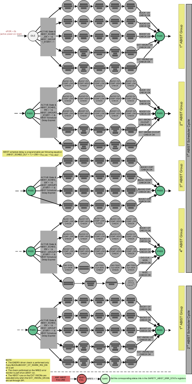
Figure 11-11 shows an example with tests for all four ABIST groups when the ABIST_GROUP1_START, ABIST_GROUP2_START, ABIST_GROPU_START3, and ABIST_GROUP_START4 control bits are set.

- ENDRV toggling is checked by the system MCU.
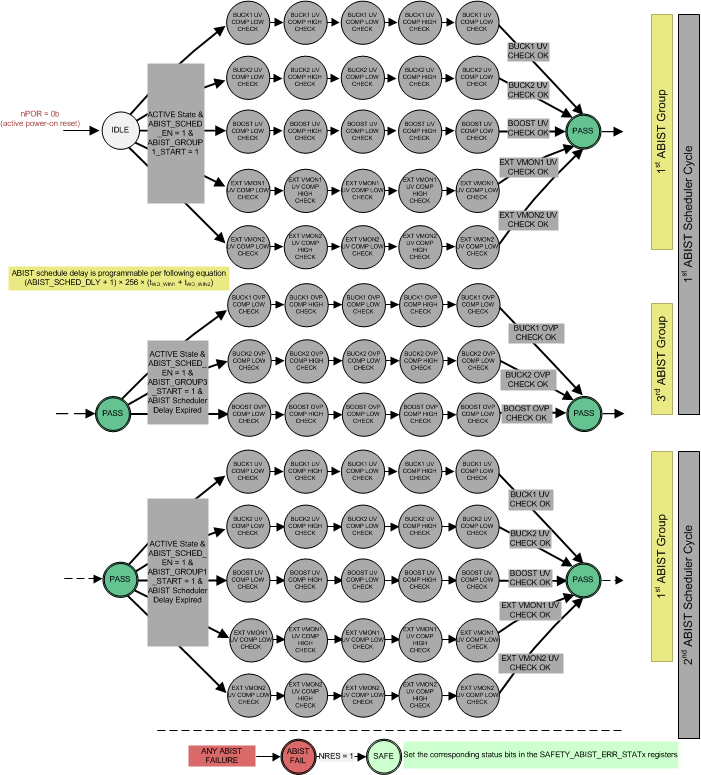
Figure 11-12 shows an example with tests for two ABIST groups when only the ABIST_GROUP1_START and ABIST_GROUP3_START control bits are set.
 Figure 11-12 ABIST Scheduler in the ACTIVE State
The ABIST scheduler runs the activated ABIST group of tests periodically in the ACTIVE state when at least one of the ABIST_GROUPx_START bits is set and while the ABIST_SCHED_EN configuration bit is set. The test repetition period is programmable through the ABIST_SCHED_DLY configuration bits in the SAFETY_CFG8 register. This time period is defined by Figure 11-10. The time delay between any two ABIST groups of tests can be from 281.6 ms to 10380.9 s.
 Figure 11-13 ABIST Scheduler
In the ACTIVE state, the t2 time interval is defined by Equation 1
where
- ABIST_SCHED_DLY is set by the configuration bits in the SAFETY_CFG8 register.
- tWD_WIN1 is a Watchdog Window #1 duration set by the configuration bits in the WDT_WIN1_CFG register.
- tWD_WIN2 is a Watchdog Window #2 duration set by the configuration bits in the WDT_WIN2_CFG register.