SLVSAY9F December   2012  – March 2016 TPS65320-Q1

PRODUCTION DATA.  

  1. Features
  2. Applications
  3. Description
  4. Revision History
  5. Pin Configuration and Functions
  6. Specifications
    1. 6.1 Absolute Maximum Ratings
    2. 6.2 ESD Ratings
    3. 6.3 Recommended Operating Conditions
    4. 6.4 Thermal Information
    5. 6.5 Electrical Characteristics
    6. 6.6 Timing Requirements
    7. 6.7 Switching Characteristics
    8. 6.8 Typical Characteristics
  7. Detailed Description
    1. 7.1 Overview
    2. 7.2 Functional Block Diagram
    3. 7.3 Feature Description
      1. 7.3.1 Buck Regulator
        1. 7.3.1.1  Fixed-Frequency PWM Control
        2. 7.3.1.2  Slope Compensation Output
        3. 7.3.1.3  Pulse-Skip Eco-mode™ Control Scheme
        4. 7.3.1.4  Dropout Operation and Bootstrap Voltage (BOOT)
        5. 7.3.1.5  Error Amplifier
        6. 7.3.1.6  Voltage Reference
        7. 7.3.1.7  Adjusting the Output Voltage
        8. 7.3.1.8  Soft-Start and Tracking Pin (SS/TR)
        9. 7.3.1.9  Overload Recovery Circuit
        10. 7.3.1.10 Constant Switching Frequency and Timing Resistor (RT/CLK Pin)
        11. 7.3.1.11 Overcurrent Protection and Frequency Shift
        12. 7.3.1.12 Selecting the Switching Frequency
        13. 7.3.1.13 How to Interface to RT/CLK Pin
        14. 7.3.1.14 Overvoltage Transient Protection
        15. 7.3.1.15 Thermal Shutdown
        16. 7.3.1.16 Small-Signal Model for Loop Response
        17. 7.3.1.17 Simple Small-Signal Model for Peak-Current Mode Control
        18. 7.3.1.18 Small-Signal Model for Frequency Compensation
      2. 7.3.2 LDO Regulator
        1. 7.3.2.1 Charge-Pump Operation
        2. 7.3.2.2 Low-Voltage Tracking
        3. 7.3.2.3 Power-Good Output, nRST
      3. 7.3.3 Enable and Undervoltage Lockout
    4. 7.4 Device Functional Modes
      1. 7.4.1 Modes of Operation
  8. Application and Implementation
    1. 8.1 Application Information
    2. 8.2 Typical Applications
      1. 8.2.1 2.2-MHz Switching Frequency, 9-V to 16-V Input, 5-V Output Buck Regulator, 3.3-V Output LDO Regulator
        1. 8.2.1.1 Design Requirements
        2. 8.2.1.2 Detailed Design Procedure
          1. 8.2.1.2.1  Switching Frequency Selection for the Buck Regulator
          2. 8.2.1.2.2  Output Inductor Selection for the Buck Regulator
          3. 8.2.1.2.3  Output Capacitor Selection for the Buck Regulator
          4. 8.2.1.2.4  Catch Diode Selection for the Buck Regulator
          5. 8.2.1.2.5  Input Capacitor Selection for the Buck Regulator
          6. 8.2.1.2.6  Soft-Start Capacitor Selection for the Buck Regulator
          7. 8.2.1.2.7  Bootstrap Capacitor Selection for the Buck Regulator
          8. 8.2.1.2.8  Output Voltage and Feedback Resistor Selection for the Buck Regulator
          9. 8.2.1.2.9  Frequency Compensation Selection for the Buck Regulator
          10. 8.2.1.2.10 LDO Regulator
          11. 8.2.1.2.11 Power Dissipation
            1. 8.2.1.2.11.1 Power Dissipation Losses of the Buck Regulator
          12. 8.2.1.2.12 Power Dissipation Losses of the LDO Regulator
          13. 8.2.1.2.13 Total Device Power Dissipation Losses and Junction Temperature
        3. 8.2.1.3 Application Curves
      2. 8.2.2 Design Example With 500-kHz Switching Frequency
        1. 8.2.2.1 Design Requirements
        2. 8.2.2.2 Detailed Design Procedure
          1. 8.2.2.2.1 Selecting the Switching Frequency
          2. 8.2.2.2.2 Output Inductor Selection
          3. 8.2.2.2.3 Output Capacitor
          4. 8.2.2.2.4 Compensation
        3. 8.2.2.3 Application Curve
  9. Power Supply Recommendations
  10. 10Layout
    1. 10.1 Layout Guidelines
      1. 10.1.1 Inductor (L)
      2. 10.1.2 Input Filter Capacitors (CI)
      3. 10.1.3 Resistive Feedback Networks
      4. 10.1.4 Traces and Ground Plane
    2. 10.2 Layout Example
  11. 11Device and Documentation Support
    1. 11.1 Device Support
      1. 11.1.1 Third-Party Products Disclaimer
    2. 11.2 Documentation Support
      1. 11.2.1 Related Documentation
    3. 11.3 Community Resource
    4. 11.4 Trademarks
    5. 11.5 Electrostatic Discharge Caution
    6. 11.6 Glossary
  12. 12Mechanical, Packaging, and Orderable Information

Package Options

Refer to the PDF data sheet for device specific package drawings

Mechanical Data (Package|Pins)
  • PWP|14
Thermal pad, mechanical data (Package|Pins)
Orderable Information

6 Specifications

6.1 Absolute Maximum Ratings

over operating free-air temperature range (unless otherwise noted)(1)
MIN MAX UNIT
Supply inputs VIN –0.3 45 V
VIN_LDO –0.3 20
VIN – VIN_LDO –0.3 45
Control EN1, EN2 –0.3 45 V
EN1-VIN, EN2-VIN 1
Buck converter FB1 –0.3 3.6 V
SW –0.3
–2 V for 30 ns
40
BOOT –0.3 46
BOOT-SW 8
COMP –0.3 3.6
SS –0.3 3.6
RT/CLK, SS –0.3 3.6
LDO regulator LDO_OUT –0.3 7 V
FB2 –0.3 7
nRST –0.3 7
Operating ambient temperature, TA –40 125 °C
Operating junction temperature, TJ –40 150
Storage temperature, Tstg –55 165 °C
(1) Stresses beyond those listed under Absolute Maximum Ratings may cause permanent damage to the device. These are stress ratings only, and functional operation of the device at these or any other conditions beyond those indicated under Recommended Operating Conditions is not implied. Exposure to absolute-maximum-rated conditions for extended periods may affect device reliability.

6.2 ESD Ratings

VALUE UNIT
V(ESD) Electrostatic discharge Human-body model (HBM), per AEC Q100-002(1) ±2000 V
Charged-device model (CDM), per AEC Q100-011 All pins ±500
Corner pins (1, 7, 8, and 14) ±750
(1) AEC Q100-002 indicates that HBM stressing shall be in accordance with the ANSI/ESDA/JEDEC JS-001 specification.

6.3 Recommended Operating Conditions

over operating free-air temperature range (unless otherwise noted)
MIN MAX UNIT
Supply inputs VIN 3.6 40 V
VIN_LDO 3 20
Buck regulator BOOT1 3.6 46 V
SW1 –1 40
VFB1 0 3
SS 0 3
COMP 0 3
RT/CLK 0 3
LDO regulator LDO_OUT 1.1 5.5 V
VFB2 0 5.25
nRST 0 5.25
Control EN1 0 40 V
EN2 0 40
Operating junction temperature, TJ –40 150 °C

6.4 Thermal Information

THERMAL METRIC(1) TPS65320-Q1 UNIT
PWP (HTSSOP)
14 PINS
RθJA Junction-to-ambient thermal resistance 49.9 °C/W
RθJC(top) Junction-to-case (top) thermal resistance 31 °C/W
RθJB Junction-to-board thermal resistance 26.6 °C/W
ψJT Junction-to-top characterization parameter 1 °C/W
ψJB Junction-to-board characterization parameter 26.4 °C/W
RθJC(bot) Junction-to-case (bottom) thermal resistance 3.7 °C/W
(1) For more information about traditional and new thermal metrics, see the Semiconductor and IC Package Thermal Metrics application report, SPRS953.

6.5 Electrical Characteristics

VI = 6 V to 27 V, EN1 = EN2 = VI, over-operating free-air temperature range TA = –40°C to +125°C and maximum operating junction temperature TJ = –40°C to +150°C, unless otherwise noted. VI is the voltage on the battery-supply pins, VIN and VIN_LDO.
PARAMETER TEST CONDITIONS MIN TYP MAX UNIT
VIN (INPUT POWER SUPPLY)
Operating input voltage Normal mode, after initial start-up 3.6 14 40 V
Shutdown supply current V(EN1) = V(EN2) = 0 V, 25°C 2 7 μA
Initial start-up voltage 6 40 V
ENABLE AND UVLO (EN1 AND EN2 PINS)
Enable low level 0.7 V
Enable high level 2.5 V
V(VIN)(f) Internal UVLO falling threshold Ramp V(VIN) down until output turns OFF 2 2.6 3 V
V(VIN)(r) Internal UVLO rising threshold Ramp V(VIN) up until output turns ON 2.2 2.8 3.2 V
BUCK REGULATOR
Operating: non-switching supply V(FB1) = 0.83 V, V(VIN) = 12 V, 25°C 110 140 μA
Output capacitor ESR = 0.001 Ω to 0.1 Ω, large output capacitance may be required for load transient 10 μF
BUCK REGULATOR: HIGH-SIDE MOSFET
On-resistance V(VIN) = 12 V, V(SW) = 6 V 127 250
BUCK REGULATOR: ERROR AMPLIFIER
Input current 50 nA
Error-amplifier transconductance (gm) –2 µA < I(COMP) < 2 µA, V(COMP) = 1 V 310 µS
Error-amplifier transconductance (gm) during soft start –2 µA < I(COMP) < 2 µA, V(COMP) = 1 V
V(FB1) = 0.4 V
70 µS
Error-amplifier dc gain V(FB1) = 0.8 V 100 dB
Error-amplifier bandwidth 6000 kHz
Error-amplifier source or sink V(COMP) = 1 V, 100-mV overdrive ±27 μA
COMP to switch-current transconductance 10.5 S
Vref1 Voltage reference for FB1 pin Buck regulator output: 3.6 V to 10 V 0.788 0.8 0.812 V
BUCK REGULATOR: CURRENT-LIMIT
Current-limit threshold V(VIN) = 12 V, TJ = 25°C 4 6 A
BUCK REGULATOR: TIMING RESISTOR AND EXTERNAL CLOCK (RT/CLK PIN)
RT/CLK High threshold 1.9 2.2 V
RT/CLK Low threshold 0.5 0.7 V
BUCK REGULATOR: INTERNAL SOFT START TIMER
IS(SS) Soft-start source current V(SS) = 0 V 1 2 4 μA
LDO REGULATOR
ΔVO(ΔVI) Line regulation V(VIN) = 6 V to 30 V, I(LDO_OUT) = 10 mA, V(LDO_OUT) = 3.3 V 20 mV
ΔVO(ΔIL) Load regulation I(LDO_OUT) = 10 mA to 200 mA, V(VIN_LDO) = 14 V, V(LDO_OUT) = 3.3 V 35 mV
VDROPOUT
(V(VIN_LDO) – V(LDO_OUT))
Dropout voltage I(LDO_OUT) = 200 mA 300 450 mV
I(LDO_OUT) Output current V(LDO_OUT) in regulation 0 280 mA
Error-amplifier dc gain 800 V/V
V(VIN_LDO) Operating input voltage on VIN_LDO pin Buck regulator is in regulation and supplying at least LDO output plus dropout voltage VDROPOUT 3 20 V
Vref2 Voltage reference for FB2 pin V(LDO_OUT) = 1.2 V to 5 V 0.788 0.8 0.812 V
ICL(LDO_OUT) Output current limit V(LDO_OUT) = 0 V (LDO_OUT pin is shorted to ground.) 280 1000 mA
IQ(LDO) Quiescent current V(VIN) > 9 V, V(EN1) = 0 V, V(EN2) = 5 V, I(LDO_OUT) = 0.01 mA to 0.75 mA, TJ = 25°C 28 75 μA
PSRR Power supply ripple rejection V(VIN_LDO)(rip) = 0.5 VPP, I(LDO_OUT) = 200 mA, frequency = 100 Hz, V(LDO_OUT) = 5 V and V(LDO_OUT) = 3.3 V 60 dB
PSRR Power supply ripple rejection VVIN_LDO(rip) = 0.5 VPP, I(LDO_OUT) = 200 mA, frequency = 150 kHz, V(LDO_OUT) = 5 V and V(LDO_OUT) = 3.3 V 30 dB
Output capacitor ESR = 0.001 Ω to 100 mΩ, large output capacitance may be required for load transient, V(LDO_OUT) ≥ 3.3 V 1 40 μF
ESR = 0.001 Ω to 100 mΩ, large output capacitance may be required for load transient, 1.2 V ≤ V(LDO_OUT) < 3.3 V 20 40 μF
LDO REGULATOR: RESET (nRST PIN)
RESET threshold V(LDO_OUT) decreasing 88% 92% 95%
VOH Output high Reset released due to rising LDO_OUT, V(LDO_OUT) ≥ 3.3 V, IOH = 100 µA –5% × V(LDO_OUT) V
VOL Output low Reset asserted due to falling LDO_OUT, IOL = 1 mA 0 0.045 0.4 V
OVERTEMPERATURE PROTECTION
TSD Thermal-shutdown trip point 155 ºC
Thys Hysteresis 10 ºC

6.6 Timing Requirements

VI = 6 V to 27 V, EN1 = EN2 = VI, over-operating free-air temperature range TA = –40°C to +125°C and maximum operating junction temperature TJ = –40°C to +150°C, unless otherwise noted
MIN TYP MAX UNIT
BUCK REGULATOR: TIMING RESISTOR AND EXTERNAL CLOCK (RT/CLK PIN)
Minimum CLK input pulse width 40 ns

6.7 Switching Characteristics

VI = 6 V to 27 V, EN1 = EN2 = VI, over-operating free-air temperature range TA = –40°C to +125°C and maximum operating junction temperature TJ = –40°C to +150°C, unless otherwise noted
PARAMETER TEST CONDITIONS MIN TYP MAX UNIT
BUCK REGULATOR: HIGH-SIDE MOSFET
tonmin Minimum on-time ƒS = 2.5 MHz 100 ns
BUCK REGULATOR: TIMING RESISTOR AND EXTERNAL CLOCK (RT/CLK PIN)
ƒS Switching-frequency range using RT mode 100 2500 kHz
ƒS Switching frequency 200 kΩ connected between pin RT/CLK and GND 450 581 720 kHz
ƒS Switching-frequency range using CLK mode 300 2200 kHz
RT/CLK Falling edge to SW rising edge delay Measured at 500 kHz with 200-kΩ series resistor connected to RT/CLK pin 60 ns
PLL Lock-in time Measured at 500 kHz 100 μs
LDO REGULATOR: RESET (nRST PIN)
Filter time Delay before asserting nRST low 6 10 15 μs

6.8 Typical Characteristics

TPS65320-Q1 C002_SLVSAY9.gif
ƒS = 2 MHz
Figure 1. Buck-Regulator Output Voltage
TPS65320-Q1 C004_SLVSAY9.gif
V(VIN) = 12 V
Figure 2. Buck-Regulator Switching Frequency vs V(FB1) Feedback Voltage
TPS65320-Q1 C003_SLVSAY9.gif
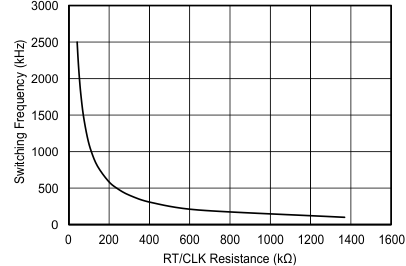
V(VIN) = 12 V TJ = 25°C
Figure 3. Buck-Regulator Switching Frequency vs RT_CLK Resistance
TPS65320-Q1 C008_SLVSAY9.gif
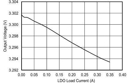
V(VIN_LDO) = 5 V V(LDO_OUT) = 3.3 V
Figure 5. LDO-Regulator Load Regulation
TPS65320-Q1 C010_SLVSAY9.gif
I(LDO_OUT) = 100 mA V(VIN_LDO) = 12 V
Figure 7. LDO-Regulator Feedback-Voltage Reference (V(FB2)) vs Junction Temperature
TPS65320-Q1 C007_SLVSAY9.gif
No Load V(VIN) = 12 V
Figure 4. Buck-Regulator Feedback-Voltage Reference (V(FB1)) vs Junction Temperature
TPS65320-Q1 C009_SLVSAY9.gif
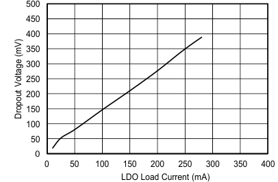
Figure 6. LDO-Regulator Dropout Voltage vs Load Current