SLVSCQ2 July 2015 TPS65400-Q1
PRODUCTION DATA.
- 1 Features
- 2 Applications
- 3 Description
- 4 Revision History
- 5 Description (continued)
- 6 Pin Configuration and Functions
- 7 Specifications
-
8 Detailed Description
- 8.1 Overview
- 8.2 Functional Block Diagrams
- 8.3
Feature Description
- 8.3.1 Startup Timing and Power Sequencing
- 8.3.2 UVLO and Precision Enables
- 8.3.3 Soft-Start and Prebiased Startup
- 8.3.4 PWM Switching Frequency Selection
- 8.3.5 Clock Synchronization
- 8.3.6 Phase Interleaving
- 8.3.7 Fault Handling
- 8.3.8 OCP for SW1 to SW4
- 8.3.9 Overcurrent Protection for SW1 to SW4 in Current Sharing Operation
- 8.3.10 Recovery on Power Loss
- 8.3.11 Feedback Compensation
- 8.3.12 Adjusting Output Voltage
- 8.3.13 Digital Interface - PMBus
- 8.3.14 Initial Configuration
- 8.4 Device Functional Modes
- 8.5
Register Maps
- 8.5.1 PMBus
- 8.5.2 PMBus Register Descriptions
- 8.5.3
PMBus Core Commands
- 8.5.3.1 (00h) PAGE
- 8.5.3.2 (01h) OPERATION
- 8.5.3.3 (03h) CLEAR_FAULTS
- 8.5.3.4 (10h) WRITE_PROTECT
- 8.5.3.5 (11h) STORE_DEFAULT_ALL
- 8.5.3.6 (19h) CAPABILITY
- 8.5.3.7 (78h) STATUS_BYTE
- 8.5.3.8 (79h) STATUS_WORD
- 8.5.3.9 (7Ah) STATUS_VOUT
- 8.5.3.10 (80h) STATUS_MFR_SPECIFIC
- 8.5.3.11 (98h) PMBUS_REVISION
- 8.5.3.12 (ADh) IC_DEVICE_ID
- 8.5.3.13 (AEh) IC_DEVICE_REV
- 8.5.4
Manufacturer-Specific Commands
- 8.5.4.1 (D0h) USER_DATA_BYTE_00
- 8.5.4.2 (D1h) USER_DATA_BYTE_01
- 8.5.4.3 (D2h) PIN_CONFIG_00
- 8.5.4.4 (D3h) PIN_CONFIG_01
- 8.5.4.5 (D4h) SEQUENCE_CONFIG
- 8.5.4.6 (D5h) SEQUENCE_ORDER
- 8.5.4.7 (D6h) IOUT_MODE
- 8.5.4.8 (D7h) FREQUENCY_PHASE
- 8.5.4.9 (D8h) VREF_COMMAND
- 8.5.4.10 (D9h) IOUT_MAX
- 8.5.4.11 (DAh) USER_RAM_00
- 8.5.4.12 (DBh) SOFT_RESET
- 8.5.4.13 (DCh) RESET_DELAY
- 8.5.4.14 (DDh) TON_TOFF_DELAY
- 8.5.4.15 (DEh) TON_TRANSITION_RATE
- 8.5.4.16 (DFh) VREF_TRANSITION_RATE
- 8.5.4.17 (F0h) SLOPE_COMPENSATION
- 8.5.4.18 (F1h) ISENSE_GAIN
- 8.5.4.19 (FCh) DEVICE_CODE
- 9 Application and Implementation
- 10Power Supply Recommendations
- 11Layout
- 12Device and Documentation Support
- 13Mechanical, Packaging, and Orderable Information
Package Options
Mechanical Data (Package|Pins)
- RGZ|48
Thermal pad, mechanical data (Package|Pins)
- RGZ|48
Orderable Information
11 Layout
11.1 Layout Guidelines
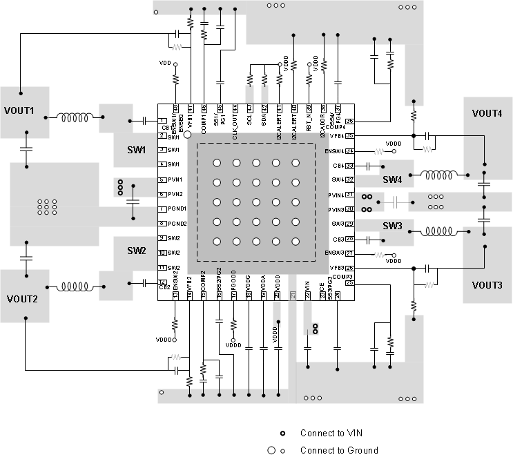
Layout is a critical portion of high-current multi-channel DC-DC. Follow these guidelines for layout. See Layout Example for a PCB layout example.
- Place VOUT and SW on the top layer and an inner power plane for VIN.
- Also on the top layer, fit connections for the remaining pins of TPS65400-Q1 and a large top-side area filled with ground.
- Connect the top layer ground area to the internal ground layer or layers using vias at the input bypass capacitor, the output filter capacitor, and directly under the TPS65400-Q1 device to provide a thermal path from the power pad to ground.
- Tie the AGND pin directly to the power pad under the IC.
- For operation at full-rated load, the top-side ground area together with the internal ground plane must provide adequate heat dissipating area.
- Several signals paths conduct fast-changing currents or voltages that can interact with stray inductance or parasitic capacitance to generate noise or degrade the power supplies' performance. To help eliminate these problems, bypass the VIN pin to ground with a low-ESR ceramic bypass capacitor with X5R or X7R dielectric. Take care to minimize the loop area formed by the bypass capacitor connections, the VIN pins, and the ground connections. Because the SW connection is the switching node, the output inductor should be located close to the SW pins, and the area of the PCB conductor minimized to prevent excessive capacitive coupling.
- The output filter capacitor ground should use the same power ground trace as the VIND input bypass capacitor. Try to minimize this conductor length while maintaining adequate width.
- The compensation should be as close as possible to the COMP pins. The COMP and ROSC pins are sensitive to noise so the components associated to these pins should be located as close as possible to the IC and routed with minimal lengths of trace.
- The VFB node is a high-impedance analog node which is easier to pick noise on board. Keep FB node trace as short as possible.
11.2 Layout Example
 Figure 46. Layout Schematic