SLVSCQ2 July 2015 TPS65400-Q1
PRODUCTION DATA.
- 1 Features
- 2 Applications
- 3 Description
- 4 Revision History
- 5 Description (continued)
- 6 Pin Configuration and Functions
- 7 Specifications
-
8 Detailed Description
- 8.1 Overview
- 8.2 Functional Block Diagrams
- 8.3
Feature Description
- 8.3.1 Startup Timing and Power Sequencing
- 8.3.2 UVLO and Precision Enables
- 8.3.3 Soft-Start and Prebiased Startup
- 8.3.4 PWM Switching Frequency Selection
- 8.3.5 Clock Synchronization
- 8.3.6 Phase Interleaving
- 8.3.7 Fault Handling
- 8.3.8 OCP for SW1 to SW4
- 8.3.9 Overcurrent Protection for SW1 to SW4 in Current Sharing Operation
- 8.3.10 Recovery on Power Loss
- 8.3.11 Feedback Compensation
- 8.3.12 Adjusting Output Voltage
- 8.3.13 Digital Interface - PMBus
- 8.3.14 Initial Configuration
- 8.4 Device Functional Modes
- 8.5
Register Maps
- 8.5.1 PMBus
- 8.5.2 PMBus Register Descriptions
- 8.5.3
PMBus Core Commands
- 8.5.3.1 (00h) PAGE
- 8.5.3.2 (01h) OPERATION
- 8.5.3.3 (03h) CLEAR_FAULTS
- 8.5.3.4 (10h) WRITE_PROTECT
- 8.5.3.5 (11h) STORE_DEFAULT_ALL
- 8.5.3.6 (19h) CAPABILITY
- 8.5.3.7 (78h) STATUS_BYTE
- 8.5.3.8 (79h) STATUS_WORD
- 8.5.3.9 (7Ah) STATUS_VOUT
- 8.5.3.10 (80h) STATUS_MFR_SPECIFIC
- 8.5.3.11 (98h) PMBUS_REVISION
- 8.5.3.12 (ADh) IC_DEVICE_ID
- 8.5.3.13 (AEh) IC_DEVICE_REV
- 8.5.4
Manufacturer-Specific Commands
- 8.5.4.1 (D0h) USER_DATA_BYTE_00
- 8.5.4.2 (D1h) USER_DATA_BYTE_01
- 8.5.4.3 (D2h) PIN_CONFIG_00
- 8.5.4.4 (D3h) PIN_CONFIG_01
- 8.5.4.5 (D4h) SEQUENCE_CONFIG
- 8.5.4.6 (D5h) SEQUENCE_ORDER
- 8.5.4.7 (D6h) IOUT_MODE
- 8.5.4.8 (D7h) FREQUENCY_PHASE
- 8.5.4.9 (D8h) VREF_COMMAND
- 8.5.4.10 (D9h) IOUT_MAX
- 8.5.4.11 (DAh) USER_RAM_00
- 8.5.4.12 (DBh) SOFT_RESET
- 8.5.4.13 (DCh) RESET_DELAY
- 8.5.4.14 (DDh) TON_TOFF_DELAY
- 8.5.4.15 (DEh) TON_TRANSITION_RATE
- 8.5.4.16 (DFh) VREF_TRANSITION_RATE
- 8.5.4.17 (F0h) SLOPE_COMPENSATION
- 8.5.4.18 (F1h) ISENSE_GAIN
- 8.5.4.19 (FCh) DEVICE_CODE
- 9 Application and Implementation
- 10Power Supply Recommendations
- 11Layout
- 12Device and Documentation Support
- 13Mechanical, Packaging, and Orderable Information
Package Options
Mechanical Data (Package|Pins)
- RGZ|48
Thermal pad, mechanical data (Package|Pins)
- RGZ|48
Orderable Information
7 Specifications
7.1 Absolute Maximum Ratings
over operating free-air temperature (unless otherwise noted) (1)| MIN | MAX | UNIT | ||
|---|---|---|---|---|
| Input voltage | PVIN1, PVIN2, PVIN3, PVIN4, VIN | –0.3 | 20 | V |
| CB1, CB2, CB3, CB4 referenced to SWx | –0.3 | 7.5 | ||
| ENSW1, ENSW2, ENSW3, ENSW4, SCL, SDA, CLK_OUT, VFB1, VFB2, VFB3, VFB4, RST_N, SCL, SDA, I2CALERT, CLK_OUT, I2CADDR, RCLOCK_SYNC | –0.3 | VDDD or 3.6 | ||
| SW1, SW2, SW3, SW4 | –1 | 20 | ||
| VDDA, VDDG | –0.3 | 7.5 | ||
| PGOOD, SS1/PG1, SS2/PG2, SS3/PG3, SS4/PG4, COMP1, COMP2, COMP3, COMP4, CE | –0.3 | VDDA or 7.5 | ||
| VDDD | –0.3 | 3.6 | ||
| TJ(max) | Junction temperature | 150 | °C | |
| Maximum lead temperature (soldering, 10 s) | 260 | °C | ||
| Tstg | Storage temperature | –65 | 150 | °C |
(1) Stresses beyond those listed under Absolute Maximum Ratings may cause permanent damage to the device. These are stress ratings only, which do not imply functional operation of the device at these or any other conditions beyond those indicated under Recommended Operating Conditions. Exposure to absolute-maximum-rated conditions for extended periods may affect device reliability.
7.2 ESD Ratings
| VALUE | UNIT | ||||
|---|---|---|---|---|---|
| V(ESD) | Electrostatic discharge | Human-body model (HBM), per AEC Q100-002(1) | ±2000 | V | |
| Charged-device model (CDM), per AEC Q100-011 | All pins | ±500 | |||
| Corner pins (1, 12, 13, 24, 25, 36, 37, and 48) | ±750 | ||||
(1) AEC Q100-002 indicates that HBM stressing shall be in accordance with the ANSI/ESDA/JEDEC JS-001 specification.
7.3 Recommended Operating Conditions
over operating free-air temperature range (unless otherwise noted)| MIN | MAX | UNIT | ||
|---|---|---|---|---|
| VIN1, VIN2, VIN3, VIN4 | Input voltage range | 4.5 | 18 | V |
| IOUT1, IOUT2 | Load current | 0 | 4 | A |
| IOUT3, IOUT4 | Load current | 0 | 2 | A |
| VFB1, VFB2, VFB3, VFB4 | Voltage feedback | 0.6 | 1.87 | V |
| TJ | Junction temperature range | –40 | 125 | °C |
7.4 Thermal Information
| THERMAL METRIC(1) | TPS65400-Q1 | UNIT | |
|---|---|---|---|
| RGZ (VQFN) | |||
| 48 PINS | |||
| RθJA | Junction-to-ambient thermal resistance | 29.8 | °C/W |
| RθJC(top) | Junction-to-case (top) thermal resistance | 14.9 | °C/W |
| RθJB | Junction-to-board thermal resistance | 6.3 | °C/W |
| ψJT | Junction-to-top characterization parameter | 0.2 | °C/W |
| ψJB | Junction-to-board characterization parameter | 6.3 | °C/W |
| RθJC(bot) | Junction-to-case (bottom) thermal resistance | 0.8 | °C/W |
(1) For more information about traditional and new thermal metrics, see the Semiconductor and IC Package Thermal Metrics application report, SPRA953.
7.5 Electrical Characteristics
VIN = 12 V, FSW = 500 kHz, TJ = –40°C to 125°C, typical values are at TJ = 25°C, unless otherwise noted| PARAMETER | TEST CONDITIONS | MIN | TYP | MAX | UNIT | |
|---|---|---|---|---|---|---|
| SWITCHER 1 AND SWITCHER 2 | ||||||
| Ilimit1, Ilimit2 | SW1, SW2 high-side current limit adjustment range | 2 | 6 | A | ||
| Ilimit-accuracy | Accuracy to nominal current limit value | Ilimit = 4 A, 5 A, 6 A | –25% | 25% | ||
| Rdson HS | SW1, SW2 HS Rds(on) | 66 | mΩ | |||
| Rdson LS | SW1, SW2 LS Rds(on) | 42 | mΩ | |||
| SWITCHER 3 AND SWITCHER 4 | ||||||
| Ilimit3, Ilimit4 | SW3 and SW4 current limit | 0.5 | 3 | A | ||
| Ilimit accuracy | Accuracy to nominal current limit value | Ilimit = 1 A, 2 A, 3 A | –25% | 25% | ||
| Rdson HS | SW3 and SW4 HS Rds(on) | 120 | mΩ | |||
| Rdson LS | SW3/4 LS Rds(on) | 90 | mΩ | |||
| FEEDBACK AND ERROR AMPLIFIERS FOR SW1 – SW4 | ||||||
| VFB | Accuracy | VREF = 1 V | –1% | 1% | ||
| VREFn | Error amplifier reference voltage | Default value | 800 | mV | ||
| VREF_STEP | I2C programmable VREF step size | 10 | mV | |||
| Gm | Error amplifier transconductance | 95 | 133 | 165 | µS | |
| Isink | Sink | 12 | µA | |||
| Isource | Source | 12 | µA | |||
| PWM SWITCHING CHARACTERISTICS | ||||||
| Phase_err12(1) | Phase error between SW1 and SW2 | Fsw = 1.1 MHz | 5⁰ | |||
| Phase_err34(1) | Phase error between SW3 and SW4 | Fsw = 1.1 MHz | 5⁰ | |||
| Fsw | Resistor-configurable PWM switching configuration | 275 | 2200 | kHz | ||
| Fsw-accuracy | PWM switching frequency accuracy | ROSC = 165 kΩ (Fsw = 1.1 MHz) |
–10% | 10% | ||
| Vrclock_sync | Voltage reference for RCLOCK_SYNC | 0.8 | V | |||
| tON_min | Lower duty cycle limit | 80 | 150 | ns | ||
| tOFF_min | Minimum off-time limit (constrains the maximum achievable duty cycle) | 150 | ns | |||
| CLOCK SYNC | ||||||
| V_HSYNC | High signal threshold | 2.6 | V | |||
| V_LSYNC | Low signal threshold | 1 | V | |||
| ICLKOUT | Max current sink/source for CLK_OUT | 2 | mA | |||
| tmin_SYNC | Minimum detectable time for sync pulse | 150 | ns | |||
| FSYNC | Frequency synchronization range | 275 | 2200 | kHz | ||
| TSYNC_DELAY | Delay between input pulse to RCLOCK_SYNC and rising edge of CLK_OUT and PWM output | 20 | ns | |||
| TIMING CHARACTERISTICS | ||||||
| trestart | Delay for restart during repeated OCP condition | 20 | ms | |||
| INTERNAL REGULATORS AND UVLO | ||||||
| VDDA | Internal subregulator output | Vin > 6.6 V | 6.1 | V | ||
| 4.5 V < Vin 6.6 V | Vin – 0.1 | |||||
| VDDD | Output of internal subregulator | 3.2 | V | |||
| VDDG | Output of Internal regulator for gate drivers | Vin > 6.6 V | 6.1 | V | ||
| 4.5 V < Vin 6.6 V | Vin – 0.1 | |||||
| IVIN | Quiescent non-switching, no load current | CE high, VFB >> VREF, (no switching) | 8 | mA | ||
| ISD | Quiescent shutdown current | CE low | 12 | 27 | µA | |
| VIN_UVLO | Input voltage UVLO | Rising | 4.25 | 4.48 | V | |
| VIN_UVLO | Input voltage UVLO | Falling | 3.4 | 3.75 | V | |
| PGOOD, ENSWx, RST_N, SSx, PG | ||||||
| R_LPGOOD | Resistance of PGOOD outputs when low | 500 | Ω | |||
| V_OLPGOOD | Logic output low voltage | I_OL = 100 µA | 0.1 | V | ||
| ISS | Soft-start current | 4.1 | 5.6 | 7.3 | µA | |
| VEN_H | Enable logic high threshold (for ENSW1, ENSW2, ENSW3, ENSW4) | VEN rising | 1.12 | 1.20 | 1.28 | V |
| VEN_L | Enable logic low threshold (for ENSW1, ENSW2, ENSW3, ENSW4) | VEN falling | 0.97 | 1.07 | V | |
| VEN_HYS | Enable hysteresis (for ENSW1, ENSW2, ENSW3, ENSW4) | 130 | mV | |||
| IEN | ENSWx pin pullup current | VEN = 0 | 2 | µA | ||
| ICE | CE pin pullup current | VCE = 0 | 2 | µA | ||
| VIH_CE | Logic input high for CE | 1.3 | V | |||
| VIL_CE | Logic input low CE | 0.4 | V | |||
| VIH_RSTN | Logic input high RST_N | 1.3 | V | |||
| VIL_RSTN | Logic input low RST_N | 0.4 | V | |||
| I2C MODULE (SDA, SCL, I2CALERT, I2CADDR) | ||||||
| V_ILI2C | Logic input low SCL, SDA | 0.8 | V | |||
| V_IHI2C | Logic input high for SCL, SDA | 2.1 | V | |||
| R_LI2C | ON resistance of I2C pins (SDA,SCL,I2CALERT) to GND | I2CALERT = 1 | 85 | Ω | ||
| V_OLI2C | Logic output low voltage for SCL,SDA,I2CALERT pins | I_OL = 350 µA | 0.1 | V | ||
| ILEAK | Input leakage current | SDA, SCL = 3.3 V | 1 | µA | ||
| II2CADDR | Source current of I2CADDR pin | VDDD = 3.3 V, VIN > 4.5 V | 20 | uA | ||
| tTIMEOUT | Timeout detection on SDA or SCL low | 30 | ms | |||
| tTIMEOUT_PULSE | Duration of timeout pulse on I2CALERT | 200 | µs | |||
| FAULTS | ||||||
| TTSD(2) | Thermal shutdown threshold | 160 | ⁰C | |||
| TTSD_restart(2) | Thermal shutdown hysteresis | 20 | ⁰C | |||
| VFB_OVP | OVP threshold rising (fault latched, PGOOD asserted) | 0.6V < VREF < 1.87 V | 111 | % of VREF | ||
| OVP threshold falling (fault cleared, PGOOD deasserted) | 0.6 V < VREF < 1.87 V | 104 | % of VREF | |||
| tOVPSDOWN | Time after OVP before protection activation and PGOOD fall | 55 | 95 | µs | ||
| VFB UVP | Undervoltage threshold (PGOOD deasserted) | 0.6 V < VREF < 1.87 V | 92 | % of VREF | ||
| Undervoltage Threshold (PGOOD asserted) | 0.6 V < VREF < 1.87 V | 83 | % of VREF | |||
| tUVPSDOWN | Time after UVP before PGOOD fall | 55 | 95 | µs | ||
(1) Specified by design.
(2) Specified by lab validation.
7.6 System Characteristics
The following specification table entries are specified by the design (component values provided in the typical application circuit are used). These parameters are not specified by production testing. Minimum and Max values apply over the full operating ambient temperature range (–40°C ≤ TJ ≤ 125°C), over the VIN range = 5 to 12 V, and IOUT range unless otherwise specified. L = 3.3 µH, DCR = 10.4 mΩ, VOUT = 1.2 V, 1% FB resistor.| PARAMETER | TEST CONDITIONS | MIN | TYP | MAX | UNIT | |
|---|---|---|---|---|---|---|
| VLINEREG | Line regulation | 0.1 | %/V | |||
| VLOADREG | Load regulation | 0.1 | %/A | |||
| tr | VOUT step duration (tr) | For 50-mV step | 30 | µs | ||
| ts | VOUT step settling time (ts) | For 50-mV step | 30 | µs | ||
| VOVUV | VOUT step overshoot/undershoot | For 50-mV step | 6 | mV | ||
| Efficiency (SW1 and SW2) | Vin = 5 V, Vo = 1.2 V, Iout = 4 A, ƒsw = 500 kHz |
77% | ||||
| Vin = 12 V, Vo = 1.2 V Iout = 4 A, ƒsw = 500 kHz |
76% | |||||
| Efficiency (SW3 and SW4) | Vin = 5 V, Vo = 1.2 V, Iout = 2 A, ƒsw= 500 kHz |
77% | ||||
| Vin = 12 V, Vo = 1.2 V Iout = 2 A, ƒsw = 500 kHz |
74% | |||||
| IOUTmatch | Average ((1)) current sharing accuracy (SW1 and SW2, SW3 and SW4) | Iload = IOUTmax | 20% | |||
| IPKmatch | Peak current ((2)) sharing accuracy (SW1 and SW2, SW3 and SW4) | Iload = IOUTmax | 20% | |||
| tacc | Timing accuracy for delays and restarts | –10% | 10% | |||
| treset_delay | Time after RSTn or CE is released for power sequence to begin | Default value | 1 | ms | ||
| treset_delay_max0 | Minimum delay after reset is released for power sequence to begin | treset_delay set to 0 ms | 1.1 | ms | ||
(1) Average current sharing accuracy is highly dependent on the matching of the inductor and capacitor.
(2) Peak current sharing accuracy refers to the max inductor current in each phase.
7.7 Operational Parameters
Values recommended that ensure proper system behavior| PARAMETER | MIN | TYP | MAX | UNIT | |
|---|---|---|---|---|---|
| CA | Stabilization capacitor to be connected to VDDA | 4.7 | µF | ||
| CD | Stabilization capacitor to be connected to VDDD | 3.3 | µF | ||
| CG | Stabilization capacitor to be connected to VDDG | 10 | µF | ||
| Vin1, Vin2, Vin3, Vin4 | SW1 to SW4 input voltage | 4.5 | 18 | V | |
| Vout1, Vout2, Vout3, Vout4 | SW1 to SW4 output voltage | 0.6 | 90% of Vin | V | |
7.8 Package Dissipation Ratings(1)
| PACKAGE | RθJA (°C/W) | TA = 25°C | TA = 55°C | TA = 85°C |
|---|---|---|---|---|
| RGZ | 29.8 | 4.5 W | 3.14 W | 1.77 W |
(1) For more information about traditional and new thermal metrics, see the Semiconductor and IC Package Thermal Metrics application report, SPRA953.
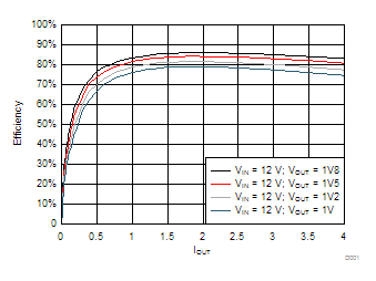
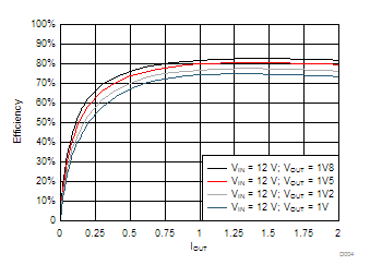
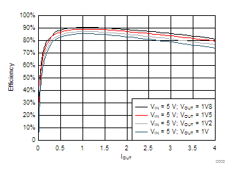
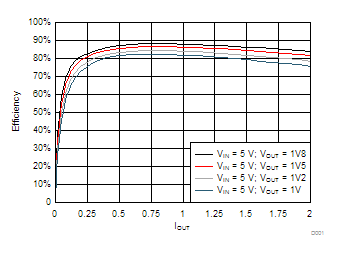
7.9 Typical Characteristics: System Efficiency

| With 500 kHz and XAL6060-472 4.7-µH, 13.2-mΩ inductor | ||

| With 500 kHz FSW and 4.7-µH, 34-mΩ inductor | ||

| With 500 kHz and XAL6060-472 4.7-µH, 13.2-mΩ inductor | ||

| With 500 kHz FSW and 4.7-µH, 34-mΩ inductor | ||