SLVSBK1E September 2012 – May 2014 TPS65631
PRODUCTION DATA.
- 1 Features
- 2 Applications
- 3 Description
- 4 Simplified Schematic
- 5 Revision History
- 6 Pin Configuration and Functions
- 7 Specifications
-
8 Detailed Description
- 8.1 Overview
- 8.2 Functional Block Diagram
- 8.3 Feature Description
- 8.4 Device Functional Modes
- 9 Applications and Implementation
- 10Power Supply Recommendations
- 11Layout
- 12Device and Documentation Support
- 13Mechanical, Packaging, and Orderable Information
Package Options
Mechanical Data (Package|Pins)
- DPD|12
Thermal pad, mechanical data (Package|Pins)
- DPD|12
Orderable Information
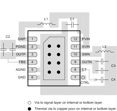
11 Layout
11.1 Layout Guidelines
No PCB layout is perfect, and compromises are always necessary. However, following the basic principles listed below (in order of importance) should go a long way to achieving good performance:
- Route switching currents on the top layer using short, wide traces. Do not route these signals through vias, which have relatively high parasitic inductance and resistance.
- Place C1 as close as possible to pin 12.
- Place C2 as close as possible to pin 3.
- Place C3 as close as possible to pin 9.
- Place L1 as close as possible to pin 1.
- Place L2 as close as possible to pin 10.
- Use the thermal pad to join GND, AGND and PGND.
- Connect the FBS pin directly to the positive pin of C2, that is, keep this connection separate from the connection between OUTP and C2.
- Use a copper pour on layer 2 as a thermal spreader and connect the thermal pad to it using a number of thermal vias.
Figure 24 illustrates how a PCB layout following the above principles may be realized in practice.