SLVSA08A February 2010 – September 2015 TPS657052
PRODUCTION DATA.
- 1 Features
- 2 Applications
- 3 Description
- 4 Revision History
- 5 Device Options
- 6 Pin Configuration and Functions
- 7 Specifications
- 8 Detailed Description
- 9 Application and Implementation
- 10Power Supply Recommendations
- 11Layout
- 12Device and Documentation Support
- 13Mechanical, Packaging, and Orderable Information
Package Options
Mechanical Data (Package|Pins)
- YZH|16
Thermal pad, mechanical data (Package|Pins)
Orderable Information
9 Application and Implementation
NOTE
Information in the following applications sections is not part of the TI component specification, and TI does not warrant its accuracy or completeness. TI’s customers are responsible for determining suitability of components for their purposes. Customers should validate and test their design implementation to confirm system functionality.
9.1 Application Information
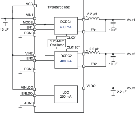
The TPS65705x device is designed for use as a power supply for embedded camera modules or other portable low-power equipment.
9.2 Typical Application

9.2.1 Design Requirements
For this design example, use the parameters listed in Table 2 as the input parameters.
Table 2. Design Parameters
| DESIGN PARAMETER | VALUE |
|---|---|
| Input Supply Voltage | 3.3 V to 6 V |
| Switching Frequency | 2.25 Mhz |
9.2.2 Detailed Design Procedure
9.2.2.1 Output Filter Design (Inductor and Output Capacitor)
9.2.2.1.1 Inductor Selection
The converter operates typically with 2.2-µH output inductor. Larger or smaller inductor values can be used to optimize the performance of the device for specific operation conditions. The selected inductor has to be rated for its DC resistance and saturation current. The DC resistance of the inductor will influence directly the efficiency of the converter. Therefore an inductor with lowest DC resistance should be selected for highest efficiency.
Equation 2 calculates the maximum inductor current under static load conditions. The saturation current of the inductor should be rated higher than the maximum inductor current as calculated with Equation 2. This is recommended because during heavy load transient the inductor current will rise above the calculated value.


where
- f = Switching Frequency (2.25 MHz typical)
- L = Inductor Value
- ΔIL = Peak-to-Peak inductor ripple current
- ILmax = Maximum Inductor current
The highest inductor current will occur at maximum Vin.
Open core inductors have a soft saturation characteristic and they can usually handle higher inductor currents versus a comparable shielded inductor.
A more conservative approach is to select the inductor current rating just for the maximum switch current of the corresponding converter. It must be considered, that the core material from inductor to inductor differs and will have an impact on the efficiency especially at high switching frequencies.
Notice that the step-down converter has internal loop compensation. As the internal loop compensation is designed to work with a certain output filter corner frequency calculated as follows:

This leads to the fact the selection of external L-C filter has to be coped with the above formula. As a general rule of thumb the product of LxCout should be constant while selecting smaller inductor or increasing output capacitor value.
Refer to Table 3 and the typical applications for possible inductors.
Table 3. Tested Inductors
| INDUCTOR TYPE | INDUCTOR VALUE | SUPPLIER |
|---|---|---|
| BRC1608 | 1.5 µH | Taiyo Yuden |
| MLP2012 | 2.2 µH | TDK |
| MIPSA2520 | 2.2 µH | FDK |
| LPS3015 | 2.2 µH | Coilcraft |
| LQM21P | 2.2 µH | Murata |
9.2.2.1.2 Output Capacitor Selection
The advanced Fast Response voltage mode control scheme of the step-down converter allows the use of small ceramic capacitors with a typical value of 10 µF, without having large output voltage under and overshoots during heavy load transients. Ceramic capacitors having low ESR values result in lowest output voltage ripple and are therefore recommended. For an inductor value of 2.2 µH, an output capacitor with 10 µF can be used. Refer to Table 4.
If ceramic output capacitors are used, the capacitor RMS ripple current rating will always meet the application requirements. Just for completeness the RMS ripple current is calculated as:

At nominal load current the inductive converters operate in PWM mode and the overall output voltage ripple is the sum of the voltage spike caused by the output capacitor ESR plus the voltage ripple caused by charging and discharging the output capacitor:

Where the highest output voltage ripple occurs at the highest input voltage Vin.
At light load currents the converter operates in Power Save Mode and the output voltage ripple is dependent on the output capacitor value. The output voltage ripple is set by the internal comparator delay and the external capacitor. The typical output voltage ripple is less than 1% of the nominal output voltage
9.2.2.1.3 Input Capacitor Selection
Because of the nature of the buck converter having a pulsating input current, a low ESR input capacitor is required for best input voltage filtering and minimizing the interference with other circuits caused by high input voltage spikes. The converters need a ceramic input capacitor of 10 µF. The input capacitor can be increased without any limit for better input voltage filtering.
Table 4. Tested Capacitors
| TYPE | COMPONENT SUPPLIER | VALUE | VOLTAGE RATING | SIZE | MATERIAL |
|---|---|---|---|---|---|
| DC-DC Output Capacitor | Murata GRM155R60G475ME47D |
4.7 µF | 4 V | 0402 | Ceramic X5R |
| LDO I/O Capacitor | Murata GRM155R60J225ME15D |
2.2 µF | 6.3 V | 0402 | Ceramic X5R |
| DC-DC Output Capacitor | Murata GRM188R60J475K |
4.7 µF | 6.3 V | 0603 | Ceramic X5R |
| DC-DC I/O Capacitor | Murata GRM188R60J106M69D |
10 µF | 6.3 V | 0603 | Ceramic X5R |
9.2.3 Application Curves
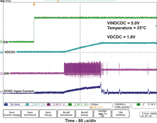
 Figure 22. Start-Up Timing DC-DC
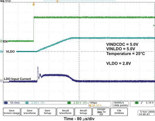
 Figure 23. Start-Up Timing LDO