SLVSBO3A December 2013 – December 2015 TPS657120
PRODUCTION DATA.
- 1 Device Overview
- 2 Revision History
- 3 Terminal Configuration and Functions
-
4 Specifications
- 4.1 Absolute Maximum Ratings
- 4.2 ESD Ratings
- 4.3 Recommended Operating Conditions
- 4.4 Thermal Information
- 4.5 Electrical Characteristics: General Functions
- 4.6 Electrical Characteristics: DCDC1 and DCDC2
- 4.7 Electrical Characteristics: DCDC3
- 4.8 Electrical Characteristics: RF-LDOs
- 4.9 Electrical Characteristics: Digital Inputs, Digital Outputs
- 4.10 Electrical Characteristics: Thermal Shutdown, Undervoltage Lockout
- 4.11 Electrical Characteristics: RFFE Timing Parameters
- 4.12 Typical Characteristics
-
5 Detailed Description
- 5.1 Overview
- 5.2 Functional Block Diagram
- 5.3
Feature Description
- 5.3.1 Default Settings
- 5.3.2 Linear Regulators
- 5.3.3 Step-down Converters DCDC1 and DCDC2
- 5.3.4 Power Save Mode
- 5.3.5 Dynamic Voltage Positioning (Optional)
- 5.3.6 Soft Start / Enable
- 5.3.7 Dynamic Voltage Scaling (DVS) for DCDC1, DCDC2 and DCDC3
- 5.3.8 100% Duty Cycle Low Dropout Operation
- 5.3.9 180° Out-of-Phase Operation
- 5.3.10 Undervoltage Lockout for DCDC1, DCDC2, DCDC3, LDO1 and LDO2
- 5.3.11 Output Voltage Discharge
- 5.3.12 Short-Circuit Protection
- 5.3.13 Output Voltage Monitoring
- 5.3.14 Step-Down Converter and LDO Enable; pins CLK_REQ1 and CLK_REQ2
- 5.3.15 Step-Down Converter DCDC3
- 5.3.16 DCDC3_SEL Control
- 5.3.17 Bypass Switch
- 5.3.18 DCDC3 Output Voltage Ramp Support
- 5.3.19 VCON Decoder
- 5.3.20 Thermal Monitoring and Shutdown
- 5.3.21 GPIOs
- 5.3.22 nRESET Input ; ADR_SELECT Input
- 5.3.23 Power State Machine
- 5.3.24 Implementation of Internal Power-Up and Power-Down Sequencing
- 5.3.25 VDDIO Voltage for Push-pull Output Stages / Interface
- 5.3.26 TPS657120 On Off Operation
- 5.3.27 MIPI RFFE Interface
- 5.4 Device Functional Modes
- 5.5 Register Maps
- 6 Application and Implementation
- 7 Power Supply Recommendations
- 8 Layout
- 9 Device and Documentation Support
- 10Mechanical, Packaging, and Orderable Information
Package Options
Mechanical Data (Package|Pins)
- YFF|30
Thermal pad, mechanical data (Package|Pins)
Orderable Information
3 Terminal Configuration and Functions
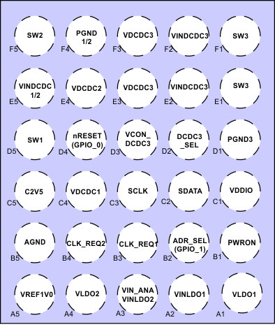
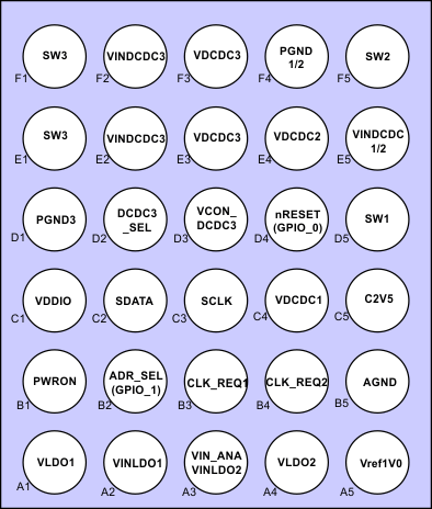
Figure 3-1 and Figure 3-2 show the 30-pin YFF Die-Size Ball-Grid Array (DSBGA) Package pin assignments.
 Figure 3-1 30-Pin YFF DSBGA (Top View)
 Figure 3-2 30-Pin YFF DSBGA (Bottom View)
3.1 Pin Attributes
Pin Attributes
| PIN | I/O | DESCRIPTION | |
|---|---|---|---|
| NAME | NO. | ||
| REFERENCE | |||
| VIN_ANA / VINLDO2 | A3 | I | Analog supply voltage input; power input for LDO2; connect to the same voltage as VINDCDC1/2 and VINDCDC3 |
| VREF1V0 | A5 | O | LDO reference bypass pin; connect a 100-nF capacitor to GND |
| C2V5 | C5 | O | Internal supply for logic; connect a 1-µF capacitor to GND |
| AGND | B5 | - | Analog ground connection; connect to PGND on the PCB |
| GPIOs | |||
| nRESET (GPIO0 ) | D4 | I/O | Primary function is active low reset input (nRESET), pin needs to be pulled to a logic HIGH per defautl in order to allow start-up. After internal configuration from OTP memory has been read, it can be assigned alternatively as general purpose I/O. Its push-pull stage is referenced to VDDIO (VIF). |
| GPIO1 (ADR_SELECT) | B2 | I/O | General purpose I/O; push-pull to VDDIO (VIF); alternatively LSB Bit address select for RFFE interface on USID[0] |
| STEP_DOWN CONVERTERS | |||
| VINDCDC1/2 | E5 | I | Power input to DCDC1 and DCDC2 converter; connect to VINDCDC3 |
| VDCDC1 | C4 | I | Voltage sense (feedback) input for DCDC1 |
| SW1 | D5 | O | Switch node of DCDC1; connect output inductor |
| PGND1/2 | F4 | - | Power GND connection for DCDC1 and DCDC2 converter |
| VDCDC2 | E4 | I | Voltage sense (feedback) input for DCDC2 |
| SW2 | F5 | O | Switch node of DCDC2; connect output inductor |
| VINDCDC3 | E2, F2 | I | Power input to DCDC3 converter and to the bypass switch; connect to VINDCDC1, VINDCDC2 and Vcc |
| VDCDC3 | E3, F3 | I | Voltage sense (feedback) input for DCDC3 and bypass output |
| SW3 | E1, F1 | O | Switch node of DCDC3; connect output inductor |
| PGND3 | D1 | - | Power GND connection for DCDC3 converter |
| LOW DROPOUT REGULATORS | |||
| VINLDO1 | A2 | I | Power input for LDO1 |
| VLDO1 | A1 | O | LDO1 output |
| VLDO2 | A4 | O | LDO2 output |
| INTERFACE | |||
| SDATA | C2 | I/O | RFFE data pin |
| SCLK | C3 | I | RFFE clock input |
| ENABLE AND CONTROL | |||
| CLK_REQ1 | B3 | I | Clock request signal1 used to enable and disable power resources |
| CLK_REQ2 | B4 | I | Clock request signal2 used to enable and disable power resources |
| DCDC3_SEL | D2 | I | Voltage scaling input to change the output voltage between two settings |
| VCON_DCDC3 | D3 | I | Analog voltage scaling input for DCDC3 |
| PWRON | B1 | I | Enable input; LOW=OFF; HIGH=ON; input voltage range up to VINDCDCx, VIN_ANA |
| VDDIO | C1 | I | Supply voltage input for GPIOs and output stages that sets the HIGH level voltage (I/O voltage); TPS657120 is held in reset if VDDIO is not in the valid range of operation |