SLVS979C October   2009  – May 2018 TPS65720 , TPS65721

PRODUCTION DATA.  

  1. Features
  2. Applications
  3. Description
    1.     Typical Application Schematic
  4. Revision History
  5. Device Options
  6. Pin Configuration and Functions
    1.     Pin Functions—DSBGA (TPS65720)
    2.     Pin Functions—DSBGA (TPS657201, TPS657202)
    3.     Pin Functions—WQFN (TPS65721)
  7. Specifications
    1. 7.1 Absolute Maximum Ratings
    2. 7.2 ESD Ratings
    3. 7.3 Recommended Operating Conditions
    4. 7.4 Thermal Information
    5. 7.5 Electrical Characteristics
    6. 7.6 Dissipation Ratings
    7. 7.7 Timing Requirements
    8. 7.8 Switching Characteristics
    9. 7.9 Typical Characteristics
  8. Detailed Description
    1. 8.1 Overview
    2. 8.2 Functional Block Diagrams
    3. 8.3 Feature Description
      1. 8.3.1  Battery Charger and Power Path
      2. 8.3.2  Power-Path Management
      3. 8.3.3  Battery Charging
        1. 8.3.3.1 I-PRECHARGE
        2. 8.3.3.2 ITERM
        3. 8.3.3.3 Battery Detection and Recharge
        4. 8.3.3.4 Charge Termination On/Off
        5. 8.3.3.5 Timers
        6. 8.3.3.6 Dynamic Timer Function
        7. 8.3.3.7 Charger Fault
      4. 8.3.4  Thermal Regulation and Thermal Shutdown
      5. 8.3.5  Battery Pack Temperature Monitoring
      6. 8.3.6  DCDC1 Converter
      7. 8.3.7  Power Save Mode
        1. 8.3.7.1 Dynamic Voltage Positioning
        2. 8.3.7.2 Soft Start
        3. 8.3.7.3 100% Duty Cycle Low Dropout Operation
        4. 8.3.7.4 Undervoltage Lockout
      8. 8.3.8  Short-Circuit Protection
      9. 8.3.9  Thermal Shutdown
      10. 8.3.10 LDO1
        1. 8.3.10.1 Default Voltage Setting for LDOs and DCDC1
        2. 8.3.10.2 Internal Analog Multiplexer (BAT, TS, TS_OUT); TPS657201, TPS657202 Only
        3. 8.3.10.3 Internal Battery Voltage Comparator
        4. 8.3.10.4 GPIOs, LED Drivers
        5. 8.3.10.5 RESET Output
        6. 8.3.10.6 Threshold Input (TPS65721 Only)
          1. 8.3.10.6.1 ENABLE for DCDC1 and LDO1
          2. 8.3.10.6.2 PB_IN Input
          3. 8.3.10.6.3 HOLD_DCDC1 Input
          4. 8.3.10.6.4 HOLD_LDO1 Input
          5. 8.3.10.6.5 INT Output
    4. 8.4 Device Functional Modes
      1. 8.4.1 Power Down
      2. 8.4.2 Sleep Mode
      3. 8.4.3 Standby Mode
      4. 8.4.4 Power-On Reset Mode
      5. 8.4.5 Idle Mode
    5. 8.5 Programming
      1. 8.5.1 Serial Interface
    6. 8.6 Register Maps
      1. 8.6.1  CHGSTATUS Register Address: 01h (read only)
      2. 8.6.2  CHGCONFIG0 Register Address: 02h (read/write)
      3. 8.6.3  CHGCONFIG1 Register Address: 03h (read/write)
      4. 8.6.4  CHGCONFIG2 Register Address: 04h (read/write)
      5. 8.6.5  CHGCONFIG3 Register Address: 05h (read/write)
      6. 8.6.6  CHGSTATE Register Address: 06h (read only)
      7. 8.6.7  DEFDCDC1 Register Address: 07h (read/write)
      8. 8.6.8  LDO_CTRL Register Address: 08h (read/write)
      9. 8.6.9  CONTROL0 Register Address: 09h (read/write)
      10. 8.6.10 CONTROL1 Register Address: 0Ah (read/write)
      11. 8.6.11 GPIO_SSC Register Address: 0Bh (read/write)
      12. 8.6.12 GPIODIR Register Address: 0Ch (read/write)
      13. 8.6.13 IRMASK0 Register Address: 0Dh (read/write)
      14. 8.6.14 IRMASK1 Register Address: 0Eh (read/write)
      15. 8.6.15 IRMASK2 Register Address: 0Fh (read/write)
      16. 8.6.16 IR0 Register Address: 10h (read only)
      17. 8.6.17 IR1 Register Address: 11h (read)
      18. 8.6.18 IR2 Register Address: 12h (read)
  9. Application and Implementation
    1. 9.1 Application Information
    2. 9.2 Typical Application
      1. 9.2.1 Design Requirements
      2. 9.2.2 Detailed Design Procedure
        1. 9.2.2.1 Output Voltage Setting
          1. 9.2.2.1.1 DCDC1
          2. 9.2.2.1.2 LDO1
        2. 9.2.2.2 Output Filter Design (Inductor and Output Capacitor)
          1. 9.2.2.2.1 Inductor Selection
          2. 9.2.2.2.2 Output Capacitor Selection
          3. 9.2.2.2.3 Input Capacitor Selection
        3. 9.2.2.3 Charger/Power Path
          1. 9.2.2.3.1 Charger Stability
          2. 9.2.2.3.2 Setting the Charge Current
          3. 9.2.2.3.3 Dynamic Power Path Management (DPPM)
      3. 9.2.3 Application Curves
  10. 10Power Supply Recommendations
  11. 11Layout
    1. 11.1 Layout Guidelines
    2. 11.2 Layout Example
  12. 12Device and Documentation Support
    1. 12.1 Device Support
      1. 12.1.1 Third-Party Products Disclaimer
    2. 12.2 Documentation Support
      1. 12.2.1 Related Documentation
    3. 12.3 Related Links
    4. 12.4 Receiving Notification of Documentation Updates
    5. 12.5 Community Resources
    6. 12.6 Trademarks
    7. 12.7 Electrostatic Discharge Caution
    8. 12.8 Glossary
  13. 13Mechanical, Packaging, and Orderable Information

Package Options

Mechanical Data (Package|Pins)
Thermal pad, mechanical data (Package|Pins)
Orderable Information

Power-Path Management

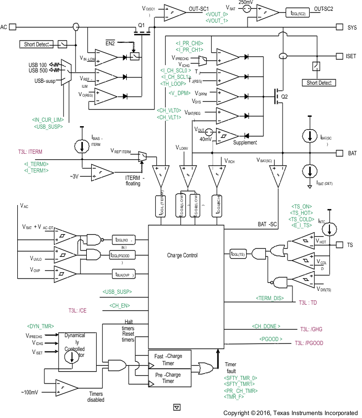
The current at the input pin AC of the power path manager is shared between charging the battery and powering the system load on the SYS pin. Priority is given to the system load. The input current is monitored continuously. If the sum of the charging and system load currents exceeds the preset maximum input current (programmed internally by I2C), the charging current is reduced automatically. The default value for the current limit is 500 mA for the AC pin.
TPS65720 TPS657201 TPS657202 TPS65721 chgr_bd_lvs979.gifFigure 10. Charger Block Diagram