SLVSAI6A June 2011 – January 2016 TPS65735
PRODUCTION DATA.
- 1 Device Overview
- 2 Revision History
- 3 Terminal Configuration and Functions
- 4 Specifications
- 5 Detailed Description
- 6 Application and Implementation
- 7 Power Supply Recommendations
- 8 Layout
- 9 Device and Documentation Support
- 10Mechanical, Packaging, and Orderable Information
Package Options
Mechanical Data (Package|Pins)
- RSN|32
Thermal pad, mechanical data (Package|Pins)
Orderable Information
5 Detailed Description
5.1 Overview
The TPS65735 integrates a linear charger and a Boost Converter to create a PMIC for active shutter 3D glasses.
5.2 Functional Block Diagram
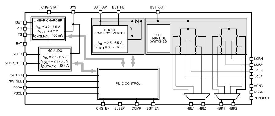 Figure 5-1 TPS65735 Simplified Functional Block Diagram
5.3 Feature Description
5.3.1 System Operation
The system must complete the power up routine before it enters normal operating mode. The specific system operation depends on the setting defined by the state of the SW_SEL pin. The details of the system operation for each configuration of the SW_SEL pin are contained in this section.
5.3.1.1 System Power Up
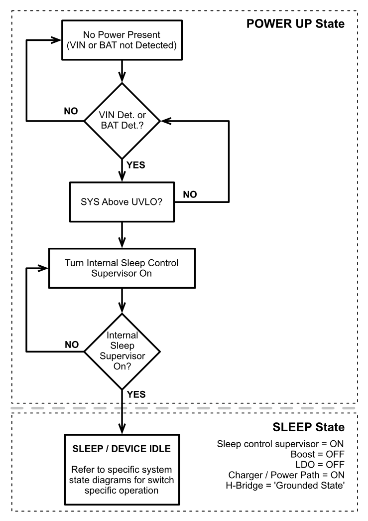 Figure 5-2 System Power Up State Diagram
5.3.1.2 System Operation Using Push Button Switch
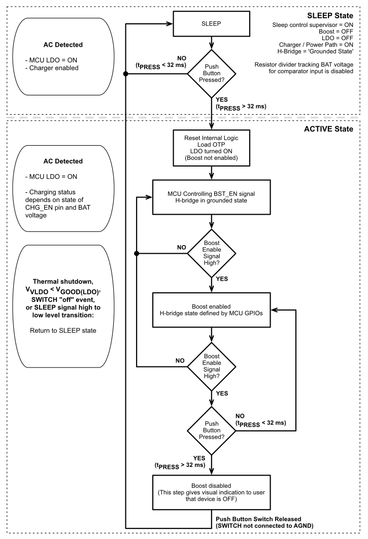 Figure 5-3 Push Button State Diagram
5.3.1.3 System Operation Using Slider Switch
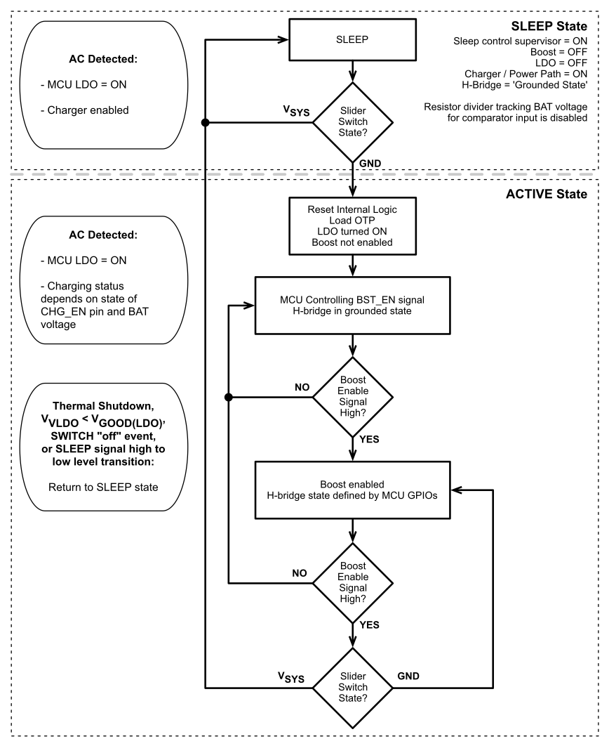 Figure 5-4 System Operation Using Slider Switch
5.3.2 Linear Charger Operation
This device has an integrated Li-Ion battery charger and system power path management feature targeted at space-limited portable applications. The architecture powers the system while simultaneously and independently charging the battery. This feature reduces the number of charge and discharge cycles on the battery, allows for proper charge termination, and enables the system to run with a defective or absent battery pack. It also allows instant system turn-on even with a totally discharged battery.
The input power source for charging the battery and running the system can be an AC adapter or USB port connected to the VIN pin as long as the input meets the device operating conditions outlined in this datasheet. The power-path management feature automatically reduces the charging current if the system load increases. Note that the charger input, VIN, has voltage protection up to 28 V.
5.3.2.1 Battery and TS Detection
To detect and determine between a good or damaged battery, the device checks for a short circuit on the BAT pin by sourcing IBAT(SC) to the battery and monitoring the voltage on the BAT pin. While sourcing this current if the BAT pin voltage exceeds VBAT(SC), a battery has been detected. If the voltage stays below the VBAT(SC) level, the battery is presumed to be damaged and not safe to charge.
The device will also check for the presence of a 10-kΩ NTC thermistor attached to the TS pin of the device. The check for the NTC thermistor on the TS pin is done much like the battery detection feature described previously. The voltage on the TS pin is compared against a defined level and if it is found to be above the threshold, the NTC thermistor is assumed to be disconnected or not used in the system. To reduce the system quiescent current, the NTC thermistor temperature sensing function is only enabled when the device is charging and when the thermistor has been detected.
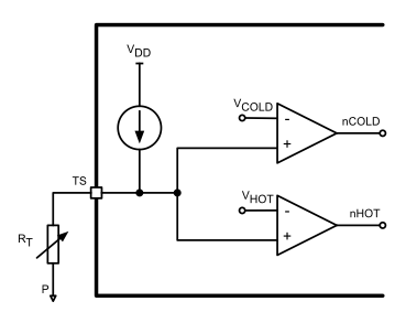 Figure 5-5 Thermistor Detection and Circuit
5.3.2.2 Battery Charging
The battery is charged in three phases: conditioning pre-charge, constant-current fast charge (current regulation), and a constant-voltage tapering (voltage regulation). In all charge phases, an internal control loop monitors the IC junction temperature and reduces the charge current if an internal temperature threshold is exceeded. Figure 5-6 shows what happens in each of the three charge phases:
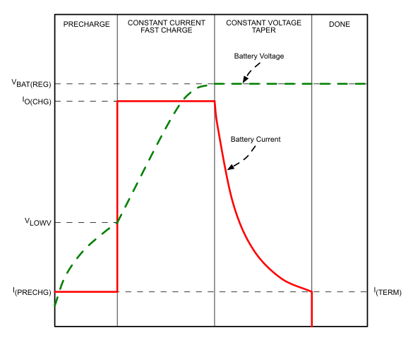 Figure 5-6 Battery Charge Phases
In the pre-charge phase, the battery is charged with the pre-charge current that is scaled to be 10% of the fast-charge current set by the resistor connected to the ISET pin. Once the battery voltage crosses the VLOWV threshold, the battery is charged with the fast-charge current (ICHG). As the battery voltage reaches VBAT(REG), the battery is held at a constant voltage of VBAT(REG) and the charge current tapers off as the battery approaches full charge. When the battery current reaches ITERM, the charger indicates charging is done by making the nCHG_STAT pin high impedance. Note that termination detection is disabled whenever the charge rate is reduced from the set point because of the actions of the thermal loop, the DPM loop, or the VIN(LOWV) loop.
5.3.2.2.1 Pre-charge
The value for the pre-charge current is set to be 10% of the charge current that is set by the external resistor, RISET. Pre-charge current is scaled to lower currents when the charger is in thermal regulation.
5.3.2.2.2 Charge Termination
In the fast charge state, once VBAT ≥ VBAT(REG), the charger enters constant voltage mode. In constant voltage mode, the charge current will taper until termination when the charge current falls below the I(TERM) threshold (typically 10% of the programmed fast charge current). Termination current is not scaled when the charger is in thermal regulation. When the charging is terminated, the nCHG_STAT pin will be high impedance (effectively turning off any LED that is connected to this pin).
5.3.2.2.3 Recharge
Once a charge cycle is complete and termination is reached, the battery voltage is monitored. If VBAT < VBAT(REG) - VRCH, the device determines if the battery has been removed. If the battery is still present, then the recharge cycle begins and will end when VBAT ≥ VBAT(REG).
5.3.2.2.4 Charge Timers
The charger in this device has internal safety timers for the pre-charge and fast charge phases to prevent potential damage to either the battery or the system. The default values for these timers are found as follows: Pre-charge timer = 0.5 hours (30 minutes) and Fast charge timer = 5 hours (300 minutes).
During the fast charge phase, the following events may increase the timer durations:
- The system load current activates the DPM loop which reduces the available charging current
- The input current is reduced because the input voltage has fallen to VIN(LOW)
- The device has entered thermal regulation because the IC junction temperature has exceeded TJ(REG)
During each of these events, the internal timers are slowed down proportionately to the reduction in charging current.
If the pre-charge timer expires before the battery voltage reaches VLOWV, the charger indicates a fault condition.
5.3.2.3 Charger Status (nCHG_STAT Pin)
The nCHG_STAT pin is used to indicate the charger status by an externally connected resistor and LED circuit. The pin is an open drain input and the internal switch is controlled by the logic inside of the charger. This pin may also be connected to a GPIO of the system MCU to indicate charging status. The table below details the status of the nCHG_STAT pin for various operating states of the charger.
Table 5-1 nCHG_STAT Functionality
| CHARGING STATUS | nCHG_STAT FET / LED | |||
|---|---|---|---|---|
| Pre-charge / Fast Charge / Charge Termination | ON | |||
| Recharge | OFF | |||
| OVP | OFF | |||
| SLEEP | OFF | |||
5.3.3 LDO Operation
The power management core has a low dropout linear regulator (LDO) with variable output voltage capability. This LDO is used for supplying the microcontroller and may be used to supply either an external IR or RF module, depending on system requirements. The LDO can supply a continuous current of up to 30 mA.
The output voltage (VVLDO) of the LDO is set by the state of the VLDO_SET pin. See Table 5-2 for details on setting the LDO output voltage.
Table 5-2 VLDO_SET Functionality
| VLDO_SET STATE | VLDO OUTPUT VOLTAGE (VVLDO) | |||
|---|---|---|---|---|
| Low (VLDO_SET < VIL(PMIC)) | 2.2 V | |||
| High (VLDO_SET > VIH(PMIC)) | 3.0 V | |||
5.3.3.1 LDO Internal Current Limit
The internal current limit feature helps protect the LDO regulator during fault conditions. During current limit, the output sources a fixed amount of current, defined in the Electrical Characteristics table. The voltage on the output in this stage can not be regulated and will be VOUT = ILIMIT × RLOAD. The pass transistor integrated into the LDO will dissipate power, (VIN - VOUT) × ILIMIT, until the device enters thermal shutdown. In thermal shutdown the device will enter the SLEEP / POWER OFF state which means that the LDO will then be disabled and shut off.
5.3.4 Boost Converter Operation
The boost converter in this device is designed for active shutter 3D glasses. This load is typically a light load where the average current is 2 mA or lower and the peak current out of a battery is limited in operation. This asynchronous boost converter operates with a minimum off time / maximum on time for the integrated low side switch, these values are specified in the Electrical Characteristics table of this datasheet.
The peak output voltage from the boost converter is adjustable and set by using an external resistor divider connected between BST_OUT pin, BST_FB pin, and ground. The peak output voltage is set by choosing resistors for the feedback network such that the voltage on the BST_FB pin is VREF(BST) = 1.2 V. See Section 6.2.1.2.2 for more information on calculating resistance values for this feedback network.
The efficiency curves for various input voltages over the typical 3D glasses load range (2 mA and lower) are shown below. All curves are for a target VOUT of 16 V. For output voltages less than 16 V, a higher efficiency at each operating input voltage should be expected. Note that efficiency is dependent upon the external boost feedback network resistance, the inductor used, and the type of load connected.
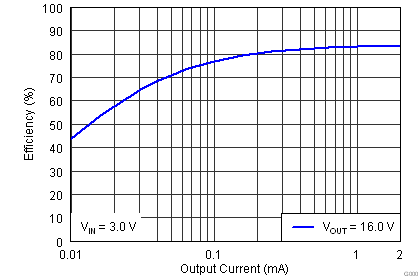
| VIN = 3.0 V | VOUT = 16 V |

| VIN = 4.2 V | VOUT = 16 V |
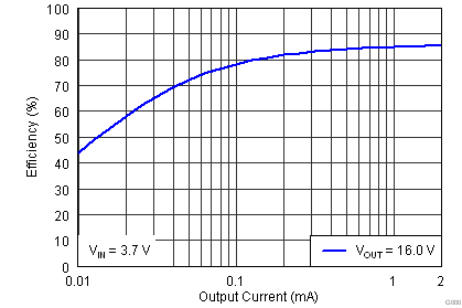
| VIN = 3.7 V | VOUT = 16 V |
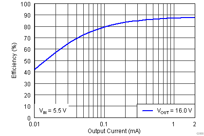
| VIN = 5.5 V | VOUT = 16 V |
5.3.4.1 Boost Thermal Shutdown
An internal thermal shutdown mode is implemented in the boost converter that shuts down the device if the typical junction temperature of 105°C is exceeded. If the device is in thermal shutdown mode, the main switch of the boost is open and the device enters the SLEEP / POWER OFF state.
5.3.4.2 Boost Load Disconnect
When the boost is disabled (BST_EN = LOW), the H-bridge is automatically placed into the OFF state. In the OFF state the high side H-bridge switches are open and the low side switches of the H-bridge are closed. The OFF state grounds and discharges the load, potentially prolonging the life of the LC shutters by eliminating any DC content (see Section 5.3.5.1 for more information regarding the H-bridge states). The disconnection of the load is done with the H-Bridge and can be seen in the next figure (Figure 5-11).
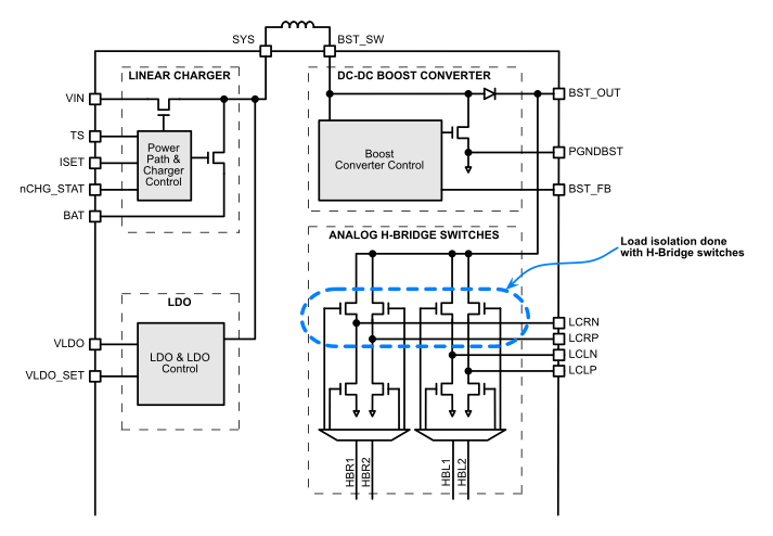 Figure 5-11 Boost Load Disconnect
An advantage to this topology for disconnecting the load is that the boost output capacitor is charged to approximately the SYS voltage level, specifically VSYS - VDIODE(BST), when the boost is disabled. This design ensures that there is not a large in-rush current into the boost output capacitor when the boost is enabled. The boost operation efficiency is also increased because there is no load disconnect switch in the boost output path. A load disconnect switch would decrease efficiency because of the resistance that it would introduce.
5.3.5 Full H-Bridge Analog Switches
The TPS65735 has two integrated full H-bridge analog switches that can be connected to GPIOs of a host microcontroller. There is an internal level shifter that manages the input signals to the H-Bridge switches.
5.3.5.1 H-Bridge Switch Control
The H-Bridge switches are controlled by an external microcontroller for system operation - specifically to control charge polarity on the LCD shutters. Depending on the state of the signals from the microcontroller, the H-Bridge will be put into 4 different states. These states are:
- OPEN: All Switches Opened
- CHARGE+: Boost Output Voltage Present on Pins LCLP or LCRP
- CHARGE-: Boost Output Voltage Present on Pins LCLN or LCRN
- GROUNDED: High Side Switches are Opened and Low Side Switches are Closed
If CHARGE+ state is followed by the CHARGE- state, the voltage across the capacitor connected to the H-Bridge output terminals will be reversed. The system automatically switches to the GROUNDED state when the boost is disabled by the BST_EN pin - for more details see Section 5.3.1.
Table 5-3 H-Bridge States from Inputs
| HBx2 [HBL2 & HBR2] | HBx1 [HBL1 & HBR1] | H-Bridge STATE | ||
|---|---|---|---|---|
| 0 | 0 | OPEN | ||
| 0 | 1 | CHARGE + | ||
| 1 | 0 | CHARGE - | ||
| 1 | 1 | GROUNDED | ||
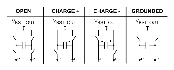 Figure 5-12 H-Bridge States
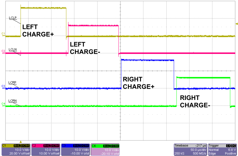 Figure 5-13 H-Bridge States from Oscilloscope
5.3.6 Power Management Core Control
Various functions of the power management core can be controlled by GPIOs of an external MCU or by setting the default state by connecting these function pins to a logic high or low level on the PCB.
5.3.6.1 SLEEP / Power Control Pin Function
The internal SLEEP signal between the power management device and the MSP430 can be used to control the power down behavior of the device. This has multiple practical applications such as a watchdog implementation for the communication between the sender (TV) and the receiver (3D glasses) or different required system on and off times; typically when the push-button press timing for an off event is a few seconds in length, programmable by software in the system MCU.
If there is a requirement that the push-button press for system on and off events are different, the SLEEP signal must be set to a logic high value (VSLEEP > VIH(PMIC)) upon system startup. This implementation allows the device to power down the system on the falling edge of the SLEEP signal
(when: VSLEEP < VIL(PMIC)).
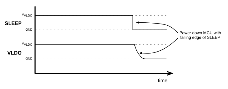 Figure 5-14 SLEEP Signal to Force System Power Off
5.3.6.2 COMP Pin Functionality
The COMP pin is used to output a scaled down voltage level related to the battery voltage for input to a comparator of a microcontroller. Applications for this COMP feature could be to generate an interrupt on the microcontroller when battery voltage drops under a threshold and the device can then be shut down or indicate to the end user with an LED that the battery requires charging.
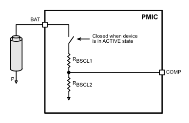 Figure 5-15 COMP Pin Internal Connection
Table 5-4 Scaling Resistors for COMP Pin Function (VVLDO = 2.2 V)
| SCALING RESISTORS FOR COMP PIN FUNCTION | VALUE | |||
|---|---|---|---|---|
| RBSCL1 | 3.0 MΩ | |||
| RBSCL2 | 2.36 MΩ | |||
Table 5-5 Scaling Resistors for COMP Pin Function (VVLDO = 3.0 V)
| SCALING RESISTORS FOR COMP PIN FUNCTION | VALUE | |||
|---|---|---|---|---|
| RBSCL1 | 3.0 MΩ | |||
| RBSCL2 | 2.48 MΩ | |||
Using the designed values in Table 5-4 or Table 5-5, the voltage on the COMP pin will be: VCOMP = 0.5 × VVLDO + 300 mV. This ensures that the COMP pin voltage will be close to half of the LDO output voltage plus the LDO dropout voltage of the device. The COMP pin can also be used as the input to an ADC channel of an external microcontroller if additional accuracy or functionality is desired over a simple comparison.
5.3.6.3 SW_SEL Pin Functionality
The SW_SEL pin is used to select what type of switch is connected to the SWITCH pin of the device. Selection between a push-button and a slider switch can be made based on the state of this pin.
Table 5-6 SW_SEL Settings
| SW_SEL STATE | TYPE OF SWITCH SELECTED | |||
|---|---|---|---|---|
| Low (VSW_SEL < VIL(PMIC)) |
Slider Switch | |||
| High (VSW_SEL > VIH(PMIC)) |
Push-button | |||
When the push button switch type is selected, the device will debounce the SWITCH input with a 32-ms timer for both the ON and OFF events and either power on or off the device. Using the push-button switch function, the ON and OFF timings are equal; tON = tOFF. If the system requirements are such that the on and off timings should be different, tON ≠ tOFF, then refer to the following section for the correct system setup: Section 6.2.1.2.3.When the slider switch operation is selected, the SWITCH pin must be externally pulled up to the SYS voltage with a resistor and the output connected to the slider switch. When the SWITCH pin is pulled to ground, the device will turn on and enter the power up sequence.
5.3.6.4 SWITCH Pin
The SWITCH pin behavior is defined by the SW_SEL pin (Section 5.3.6.3) which defines the type of switch that is connected to the system; either a slider switch or push-button.
5.3.6.5 Slider Switch Behavior
If a slider switch is connected in the system then the system power state and VLDO output (which can power an external MCU) is defined by the state of the slider switch. If the slider is in the off position than the SWITCH pin should be connected to the SYS pin. If the slider is in the on position than the SWITCH pin should be connected to ground. Figure 5-16 details the system operation using the slider switch configuration.
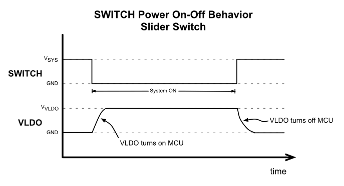 Figure 5-16 SWITCH, Slider Power On-Off Behavior
5.3.6.6 Push-Button Switch Behavior
The system is powered on or off by a push-button press after a press that is greater than 32 ms. The following figures (Figure 5-17 and Figure 5-18) show the system behavior and the expected VLDO output during the normal push-button operation where the ON and OFF press timings are the same value,
tON = tOFF.
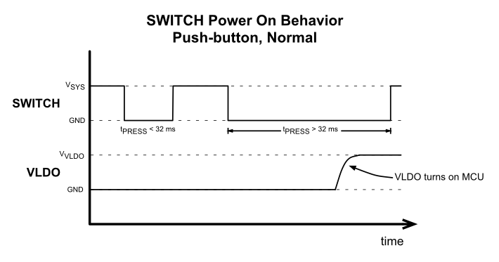 Figure 5-17 SWITCH, Push-button Power On Behavior
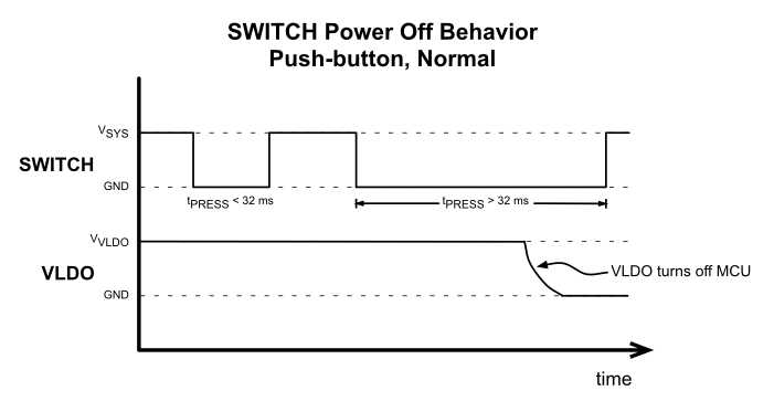 Figure 5-18 SWITCH, Push-Button Power Off Behavior
5.4 Device Functional Modes
5.4.1 SLEEP State
If the device is in the SLEEP State or Device IDLE mode, the Sleep control supervisor and the battery charger/power path remain active. The Boost and LDO are disabled.
5.4.2 NORMAL Operating Mode
Once the system completes the power up routine, it enters the normal operating mode. The specific system operation is set by the SW_SEL pin.