SLVSAI6A June   2011  – January 2016 TPS65735

PRODUCTION DATA.  

  1. Device Overview
    1. 1.1 Features
    2. 1.2 Applications
    3. 1.3 Description
    4. 1.4 Functional Block Diagram
  2. Revision History
  3. Terminal Configuration and Functions
    1. 3.1 Pin Diagram
    2. 3.2 Pin Functions
  4. Specifications
    1. 4.1 Absolute Maximum Ratings
    2. 4.2 ESD Ratings
    3. 4.3 Power-On Hours (POH)
    4. 4.4 Recommended Operating Conditions
    5. 4.5 Thermal Information
    6. 4.6 Electrical Characteristics
    7. 4.7 Quiescent Current
    8. 4.8 Typical Characteristics
  5. Detailed Description
    1. 5.1 Overview
    2. 5.2 Functional Block Diagram
    3. 5.3 Feature Description
      1. 5.3.1 System Operation
        1. 5.3.1.1 System Power Up
        2. 5.3.1.2 System Operation Using Push Button Switch
        3. 5.3.1.3 System Operation Using Slider Switch
      2. 5.3.2 Linear Charger Operation
        1. 5.3.2.1 Battery and TS Detection
        2. 5.3.2.2 Battery Charging
          1. 5.3.2.2.1 Pre-charge
          2. 5.3.2.2.2 Charge Termination
          3. 5.3.2.2.3 Recharge
          4. 5.3.2.2.4 Charge Timers
        3. 5.3.2.3 Charger Status (nCHG_STAT Pin)
      3. 5.3.3 LDO Operation
        1. 5.3.3.1 LDO Internal Current Limit
      4. 5.3.4 Boost Converter Operation
        1. 5.3.4.1 Boost Thermal Shutdown
        2. 5.3.4.2 Boost Load Disconnect
      5. 5.3.5 Full H-Bridge Analog Switches
        1. 5.3.5.1 H-Bridge Switch Control
      6. 5.3.6 Power Management Core Control
        1. 5.3.6.1 SLEEP / Power Control Pin Function
        2. 5.3.6.2 COMP Pin Functionality
        3. 5.3.6.3 SW_SEL Pin Functionality
        4. 5.3.6.4 SWITCH Pin
        5. 5.3.6.5 Slider Switch Behavior
        6. 5.3.6.6 Push-Button Switch Behavior
    4. 5.4 Device Functional Modes
      1. 5.4.1 SLEEP State
      2. 5.4.2 NORMAL Operating Mode
  6. Application and Implementation
    1. 6.1 Application Information
    2. 6.2 Typical Application
      1. 6.2.1 Active Shutter 3D Glasses
        1. 6.2.1.1 Design Requirements
        2. 6.2.1.2 Detailed Design Procedure
          1. 6.2.1.2.1 Reducing System Quiescent Current (IQ)
          2. 6.2.1.2.2 Boost Converter Application Information
            1. 6.2.1.2.2.1 Setting Boost Output Voltage
            2. 6.2.1.2.2.2 Boost Inductor Selection
            3. 6.2.1.2.2.3 Boost Capacitor Selection
          3. 6.2.1.2.3 Bypassing Default Push-Button SWITCH Functionality
        3. 6.2.1.3 Application Curves
  7. Power Supply Recommendations
  8. Layout
    1. 8.1 Layout Guidelines
    2. 8.2 Layout Example
  9. Device and Documentation Support
    1. 9.1 Device Support
      1. 9.1.1 Third-Party Products Disclaimer
    2. 9.2 Community Resources
    3. 9.3 Trademarks
    4. 9.4 Electrostatic Discharge Caution
    5. 9.5 Glossary
  10. 10Mechanical, Packaging, and Orderable Information
    1. 10.1 Packaging Information

Package Options

Mechanical Data (Package|Pins)
Thermal pad, mechanical data (Package|Pins)
Orderable Information

8 Layout

8.1 Layout Guidelines

The layout is an important step in the design process. Proper function of the device demands careful attention to the PCB layout. Care must be taken in board layout to get the specified performance. If the layout is not carefully done, the regulators may show poor performance including stability issues as well as EMI problems. It is critical to provide a low impedance ground path. Therefore, use wide and short traces for the main current paths. The input capacitors must be placed as close as possible to the IC pins as well as the inductor and output capacitor.

Keep the common path to the ground pins which return the small signal components and the high current of the output capacitors as short as possible in order to avoid ground noise.

8.2 Layout Example
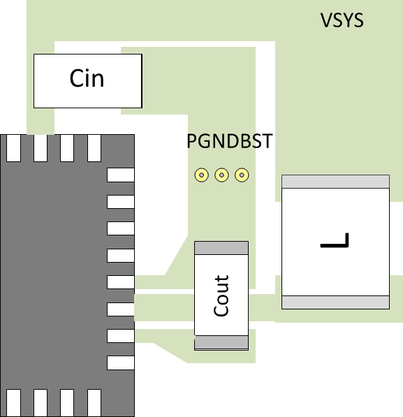
TPS65735 BST_Layout.gif Figure 8-1 Boost Layout