SLVSAF6A June 2011 – January 2016 TPS65835
PRODUCTION DATA.
- 1 Device Overview
- 2 Revision History
- 3 Terminal Configuration and Functions
- 4 Specifications
-
5 Detailed Description
- 5.1 Overview
- 5.2 Functional Block Diagram
- 5.3 Feature Description
- 5.4 Device Functional Modes
- 5.5
MSP430 CORE
- 5.5.1
MSP430 Electrical Characteristics
- 5.5.1.1 MSP430 Recommended Operating Conditions
- 5.5.1.2 Active Mode Supply Current Into VCC Excluding External Current
- 5.5.1.3 Typical Characteristics, Active Mode Supply Current (Into VCC)
- 5.5.1.4 Low-Power Mode Supply Currents (Into VCC) Excluding External Current
- 5.5.1.5 Typical Characteristics, Low-Power Mode Supply Currents
- 5.5.1.6 Schmitt-Trigger Inputs, Ports Px
- 5.5.1.7 Leakage Current, Ports Px
- 5.5.1.8 Outputs, Ports Px
- 5.5.1.9 Output Frequency, Ports Px
- 5.5.1.10 Typical Characteristics, Outputs
- 5.5.1.11 Pin-Oscillator Frequency - Ports Px
- 5.5.1.12 Typical Characteristics, Pin-Oscillator Frequency
- 5.5.1.13 POR/Brownout Reset (BOR)
- 5.5.1.14 Typical Characteristics, POR/Brownout Reset (BOR)
- 5.5.1.15 DCO Frequency
- 5.5.1.16 Calibrated DCO Frequencies, Tolerance
- 5.5.1.17 Wake-Up From Lower-Power Modes (LPM3/4)
- 5.5.1.18 Typical Characteristics, DCO Clock Wake-Up Time From LPM3/4
- 5.5.1.19 Crystal Oscillator, XT1, Low-Frequency Mode
- 5.5.1.20 Internal Very-Low-Power Low-Frequency Oscillator (VLO)
- 5.5.1.21 Timer_A
- 5.5.1.22 USCI (UART Mode)
- 5.5.1.23 USCI (SPI Master Mode)
- 5.5.1.24 USCI (SPI Slave Mode)
- 5.5.1.25 USCI (I2C Mode)
- 5.5.1.26 Comparator_A+
- 5.5.1.27 Typical Characteristics - Comparator_A+
- 5.5.1.28 10-Bit ADC, Power Supply and Input Range Conditions
- 5.5.1.29 10-Bit ADC, Built-In Voltage Reference
- 5.5.1.30 10-Bit ADC, External Reference
- 5.5.1.31 10-Bit ADC, Timing Parameters
- 5.5.1.32 10-Bit ADC, Linearity Parameters
- 5.5.1.33 10-Bit ADC, Temperature Sensor and Built-In VMID
- 5.5.1.34 Flash Memory
- 5.5.1.35 RAM
- 5.5.1.36 JTAG and Spy-Bi-Wire Interface
- 5.5.1.37 JTAG Fuse
- 5.5.2 MSP430 Core Operation
- 5.5.1
MSP430 Electrical Characteristics
- 6 Application and Implementation
- 7 Power Supply Recommendations
- 8 Layout
- 9 Device and Documentation Support
- 10Mechanical, Packaging, and Orderable Information
Package Options
Mechanical Data (Package|Pins)
- RKP|40
Thermal pad, mechanical data (Package|Pins)
- RKP|40
Orderable Information
6 Application and Implementation
NOTE
Information in the following applications sections is not part of the TI component specification, and TI does not warrant its accuracy or completeness. TI’s customers are responsible for determining suitability of components for their purposes. Customers should validate and test their design implementation to confirm system functionality.
6.1 Application Information
This PMIC is designed specifically for active shutter 3D glasses.
6.2 Typical Application
6.2.1 Active Shutter 3D Glasses
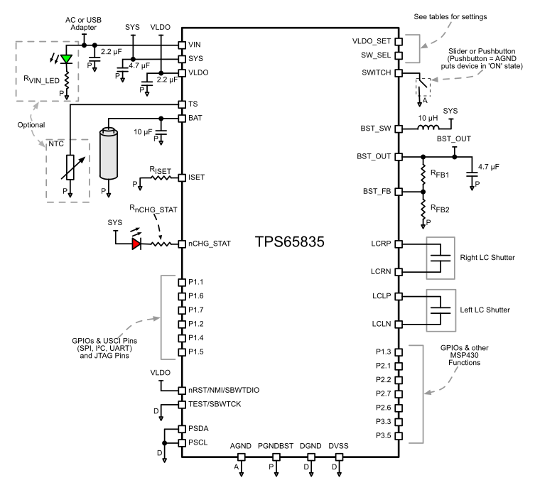 Figure 6-1 TPS65835 Applications Schematic
6.2.1.1 Design Requirements
The design parameters are located in Table 6-1.
Table 6-1 Design Parameters
| PARAMETER | EXAMPLE |
|---|---|
| Input Voltage, VIN | 3.7 to 6.4 V |
| Input Voltage, Vbat BAT | 2.5 to 6.4 V |
| Output Voltage, LDO VLDO | 2.2 (default) or 3.0 V |
| Output Voltage Boost, BST_OUT | 8 to 16 V, 10 V default |
| Charge Current Ichg=Kiset/Riset | 5 to 100 mA, 70 mA default |
| Input Voltage Low VIL
(BST_EN, CHG_EN, SW_SEL, VLDO, HBRx, HBLx) |
0.4 V |
| Input Voltage High VIH
(BST_EN, CHG_EN, SW_SEL, VLDO, HBRx, HBLx) |
1.2 V |
6.2.1.2 Detailed Design Procedure
6.2.1.2.1 Boost Converter Application Information
6.2.1.2.1.1 Setting Boost Output Voltage
To set the boost converter output voltage of this device, two external resistors that form a feedback network are required. The values recommended below (in Table 6-2) are given for a desired quiescent current of 5 µA when the boost is enabled and switching. See Figure 6-2 for the detail of the applications schematic that shows the boost feedback network and the resistor names used in the table below.
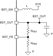 Figure 6-2 Boost Feedback Network Schematic
Table 6-2 Recommended RFB1 and RFB2 Values (for IQ(FB) = 5 µA)
| TARGETED VBST_OUT | RFB1(1) | RFB2(1) | ||
|---|---|---|---|---|
| 8 V | 1.3 MΩ | 240 kΩ | ||
| 10 V | 1.8 MΩ | 240 kΩ | ||
| 12 V | 2.2 MΩ | 240 kΩ | ||
| 14 V | 2.4 MΩ | 240 kΩ | ||
| 16 V | 3.0 MΩ | 240 kΩ | ||
These resistance values can also be calculated using the following information. To start, it is helpful to target a quiescent current through the boost feedback network while the device is operating (IQ(FB)). When the boost output voltage and this targeted quiescent current is known, the total feedback network resistance can be found.
The value for RFB2 can be found by using the boost feedback pin voltage (VFB = 1.2 V, see Section 4.6) and IQ(FB) using Equation 1:
To find RFB1, simply subtract the RFB2 from RFB(TOT) as shown in Equation 3.
6.2.1.2.1.2 Boost Inductor Selection
The selection of the boost inductor and output capacitor is very important to the performance of the boost converter. The boost has been designed for optimized operation when a 10 µH inductor is used. Smaller inductors, down to 4.7 µH, may be used but there will be a slight loss in overall operating efficiency. A few inductors that have been tested and found to give good performance can be found in the following list.
Recommended 10-µH inductors:
- TDK VLS201612ET-100M (10 µH, IMAX = 0.53 A, RDC = 0.85 Ω)
- Taiyo Yuden CBC2016B100M (10 µH, IMAX = 0.41 A, RDC = 0.82 Ω)
6.2.1.2.1.3 Boost Capacitor Selection
The recommended minimum value for the capacitor on the boost output, BST_OUT pin, is 4.7 µF. Values that are larger can be used with the measurable impact being a slight reduction in the boost converter output voltage ripple while values smaller than this will result in an increased boost output voltage ripple. Note that the voltage rating of the capacitor should be sized for the maximum expected voltage at the BST_OUT pin.
6.2.1.2.2 Bypassing Default Push-Button SWITCH Functionality
If the SWITCH pin functionality is not required to power on and off the device because of different system requirements (SWITCH timing requirements of system will be controlled by the internal MSP430), then the feature can be bypassed. The following diagram shows the connections required for this configuration.
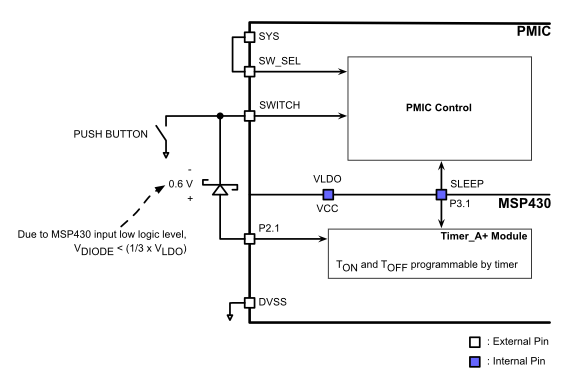 Figure 6-3 Bypassing Default TPS65835 Push Button SWITCH Timing
In a system where a different push-button SWITCH off timing is required, the SLEEP pin is used to control the power off of the device. After system power up, the MCU must force the SLEEP pin to a high state (VSLEEP > VIH(PMIC)). Once the SWITCH push-button is pressed to shut the system down, a timer in the MCU should be active and counting the desired tOFF time of the device. Once this tOFF time is detected, the MCU can assert the SLEEP signal to a logic low level (VSLEEP < VIL(PMIC)). It is on the falling edge of the SLEEP signal where the system will be powered off (see Figure 6-4).
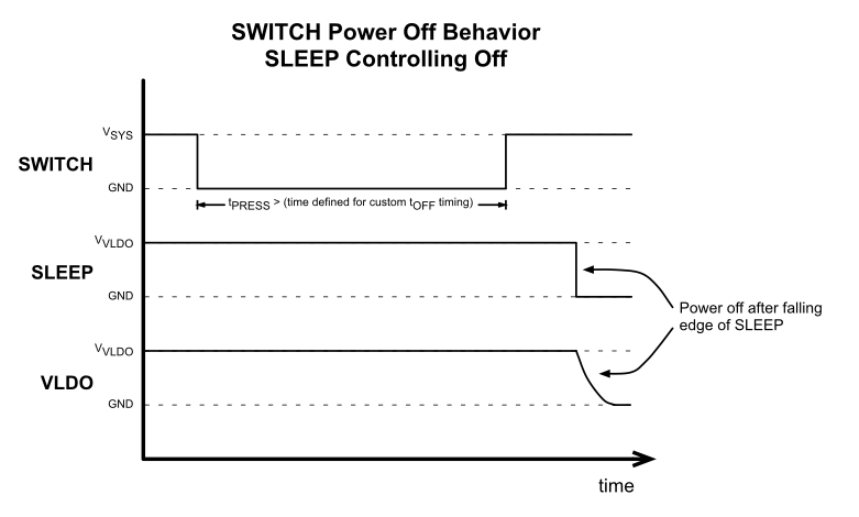 Figure 6-4 SWITCH Press and SLEEP Signal to Control System Power Off
6.2.1.2.3 MSP430 Programming
In order to program the integrated MSP430 in the TPS65835 device, ensure that the programming environment supports the TPS65835 device.
6.2.1.2.3.1 Code To Setup Power Functions
This section will detail a basic code to control the MSP430 in the TPS65835 and how to configure the power functions and control the power die. Please reference Table 5-9 for the details on configuring the MSP430 pins. Note that "//" is a comment and this code was written using Code Composer Studio in C.
// SETUP H-BRIDGE PINS
P2DIR |= (BIT5 + BIT4 + BIT3 + BIT0);  // Set PxDIR to 1 for outputs
P2REN |= (BIT5 + BIT4 + BIT3 + BIT0);  // Enable pull-up/pull-down resistors on outputs

// SETUP SLEEP, CHG_EN, AND BST_EN
P3DIR |= (BIT2 + BIT1 + BIT0);         // Set PxDIR to 1 for outputs
P3REN |= (BIT2 + BIT1 + BIT0);         // Enable pull-up/pull-down resistors on outputs
The previous code setup the power pins for outputs, now they must be controlled with MSP430 code. Refer to the following code to perform initial setup and to control the power functions (SLEEP, CHG_EN, and BST_EN):
P3OUT &= ~BIT0;        // Set SLEEP mode signal low; SLEEP Function is disabled
// P3OUT |= BIT0;      // Set SLEEP mode signal high (sleep control via MSP430)

// P3OUT &= ~BIT1;     // Set CHG_EN signal low (disable charger)
P3OUT |= BIT1;         // Set CHG_EN signal high (enable charger)

// P3OUT &= ~BIT2;     // Set BST_EN low (disable boost)
P3OUT |= BIT2;         // Set BST_EN high (enable boost)
The H-Bridge pins can be controlled in a similar manner (see Section 5.3.5.1). The following code is only meant to cover each H-Bridge mode of operation and the appropriate code needed to put it in that state:
// BOTH SIDES IN OPEN STATE
P2OUT &= ~(BIT3 + BIT0);           // HBL2 = 0, HBL1 = 0
P2OUT &= ~(BIT5 + BIT4);           // HBR2 = 0, HBR1 = 0

// BOTH SIDES IN GROUNDED STATE
P2OUT |= BIT3 + BIT0;              // HBL2 = 1, HBL1 = 1
P2OUT |= BIT5 + BIT4;              // HBR2 = 1, HBR1 = 1

// LEFT SIDE IN CHARGE+ STATE
P2OUT &= ~BIT3; P2OUT |= BIT0;     // HBL2 = 0, HBL1 = 1

// LEFT SIDE IN CHARGE- STATE
P2OUT |= BIT3; P2OUT &= ~BIT0;     // HBL2 = 1, HBL1 = 0

// RIGHT SIDE IN CHARGE+ STATE
P2OUT &= ~BIT5; P2OUT |= BIT4;     // HBR2 = 0, HBR1 = 1

// RIGHT SIDE IN CHARGE- STATE
P2OUT |= BIT5; P2OUT &= ~BIT4;     // HBR2 = 1, HBR1 = 0
6.2.1.3 Application Curves
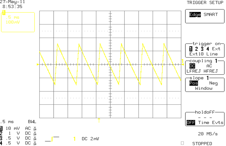
| Vbat = –3.2 V | 1-mA Load on Boost |
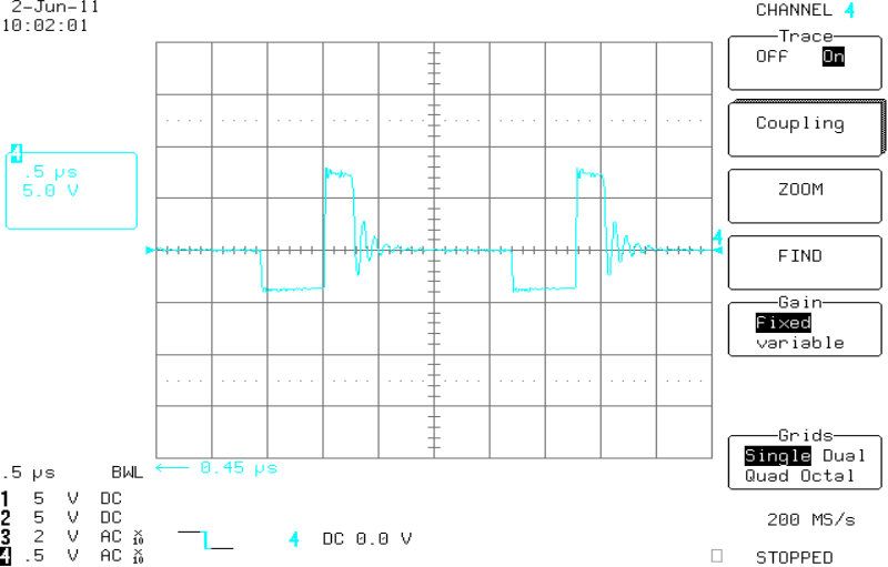
| Vbat = 3.6 V | No Load | 0.5 µs/div |