SLVSAF6A June 2011 – January 2016 TPS65835
PRODUCTION DATA.
- 1 Device Overview
- 2 Revision History
- 3 Terminal Configuration and Functions
- 4 Specifications
-
5 Detailed Description
- 5.1 Overview
- 5.2 Functional Block Diagram
- 5.3 Feature Description
- 5.4 Device Functional Modes
- 5.5
MSP430 CORE
- 5.5.1
MSP430 Electrical Characteristics
- 5.5.1.1 MSP430 Recommended Operating Conditions
- 5.5.1.2 Active Mode Supply Current Into VCC Excluding External Current
- 5.5.1.3 Typical Characteristics, Active Mode Supply Current (Into VCC)
- 5.5.1.4 Low-Power Mode Supply Currents (Into VCC) Excluding External Current
- 5.5.1.5 Typical Characteristics, Low-Power Mode Supply Currents
- 5.5.1.6 Schmitt-Trigger Inputs, Ports Px
- 5.5.1.7 Leakage Current, Ports Px
- 5.5.1.8 Outputs, Ports Px
- 5.5.1.9 Output Frequency, Ports Px
- 5.5.1.10 Typical Characteristics, Outputs
- 5.5.1.11 Pin-Oscillator Frequency - Ports Px
- 5.5.1.12 Typical Characteristics, Pin-Oscillator Frequency
- 5.5.1.13 POR/Brownout Reset (BOR)
- 5.5.1.14 Typical Characteristics, POR/Brownout Reset (BOR)
- 5.5.1.15 DCO Frequency
- 5.5.1.16 Calibrated DCO Frequencies, Tolerance
- 5.5.1.17 Wake-Up From Lower-Power Modes (LPM3/4)
- 5.5.1.18 Typical Characteristics, DCO Clock Wake-Up Time From LPM3/4
- 5.5.1.19 Crystal Oscillator, XT1, Low-Frequency Mode
- 5.5.1.20 Internal Very-Low-Power Low-Frequency Oscillator (VLO)
- 5.5.1.21 Timer_A
- 5.5.1.22 USCI (UART Mode)
- 5.5.1.23 USCI (SPI Master Mode)
- 5.5.1.24 USCI (SPI Slave Mode)
- 5.5.1.25 USCI (I2C Mode)
- 5.5.1.26 Comparator_A+
- 5.5.1.27 Typical Characteristics - Comparator_A+
- 5.5.1.28 10-Bit ADC, Power Supply and Input Range Conditions
- 5.5.1.29 10-Bit ADC, Built-In Voltage Reference
- 5.5.1.30 10-Bit ADC, External Reference
- 5.5.1.31 10-Bit ADC, Timing Parameters
- 5.5.1.32 10-Bit ADC, Linearity Parameters
- 5.5.1.33 10-Bit ADC, Temperature Sensor and Built-In VMID
- 5.5.1.34 Flash Memory
- 5.5.1.35 RAM
- 5.5.1.36 JTAG and Spy-Bi-Wire Interface
- 5.5.1.37 JTAG Fuse
- 5.5.2 MSP430 Core Operation
- 5.5.1
MSP430 Electrical Characteristics
- 6 Application and Implementation
- 7 Power Supply Recommendations
- 8 Layout
- 9 Device and Documentation Support
- 10Mechanical, Packaging, and Orderable Information
Package Options
Mechanical Data (Package|Pins)
- RKP|40
Thermal pad, mechanical data (Package|Pins)
- RKP|40
Orderable Information
8 Layout
8.1 Layout Guidelines
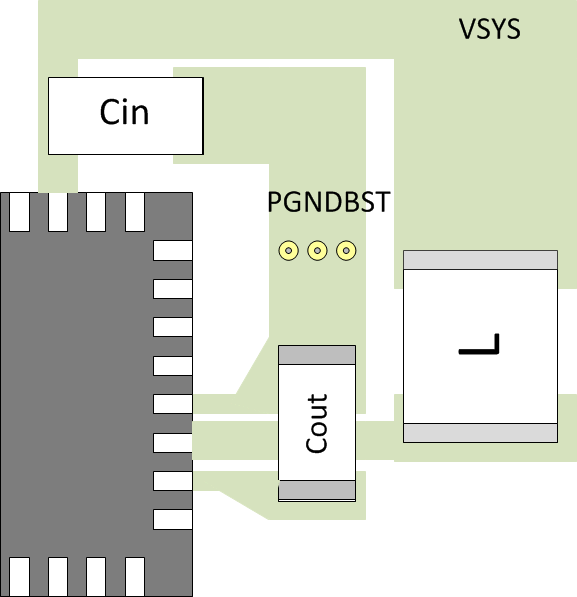
The layout is an important step in the design process. Proper function of the device demands careful attention to the PCB layout. Care must be taken in board layout to get the specified performance. If the layout is not carefully done, the regulators may show poor performance including stability issues as well as EMI problems. It is critical to provide a low impedance ground path. Therefore, use wide and short traces for the main current paths. The input capacitors must be placed as close as possible to the IC pins as well as the inductor and output capacitor.
Keep the common path to the ground pins which return the small signal components and the high current of the output capacitors as short as possible in order to avoid ground noise.
8.2 Layout Example
 Figure 8-1 Boost Layout