SWCS106F March   2013  – July 2016 TPS659119-Q1

PRODUCTION DATA.  

  1. Features
  2. Applications
  3. Description
  4. Revision History
  5. Description (continued)
  6. Pin Configuration and Functions
  7. Specifications
    1. 7.1  Absolute Maximum Ratings
    2. 7.2  ESD Ratings
    3. 7.3  Recommended Operating Conditions
    4. 7.4  Thermal Characteristics
    5. 7.5  External Component Recommendation
    6. 7.6  I/O Pullup and Pulldown Characteristics
    7. 7.7  Digital I/O Voltage Electrical Characteristics
    8. 7.8  I2C Interface and Control Signals
    9. 7.9  Switching Characteristics—I2C Interface and Control Signals
    10. 7.10 Power Consumption
    11. 7.11 Power References and Thresholds
    12. 7.12 Thermal Monitoring and Shutdown
    13. 7.13 32-kHz RTC Clock
    14. 7.14 VRTC LDO
    15. 7.15 VIO SMPS
    16. 7.16 VDD1 SMPS
    17. 7.17 VDD2 SMPS
    18. 7.18 EXTCTRL
    19. 7.19 LDO1 AND LDO2
    20. 7.20 LDO3 and LDO4
    21. 7.21 LDO5
    22. 7.22 LDO6 and LDO7
    23. 7.23 LDO8
    24. 7.24 Timing Requirements for Boot Sequence Example
    25. 7.25 Power Control Timing Requirements
    26. 7.26 Device SLEEP State Control Timing Requirements
    27. 7.27 Supplies State Control Through EN1 and EN2 Timing Characteristics
    28. 7.28 VDD1 Supply Voltage Control Through EN1 Timing Requirements
    29. 7.29 Typical Characteristics
      1. 7.29.1 VIO SMPS Curves
      2. 7.29.2 VDD1 SMPS Curves
      3. 7.29.3 VDD2 SMPS Curves
  8. Detailed Description
    1. 8.1 Overview
    2. 8.2 Functional Block Diagram
    3. 8.3 Feature Description
      1. 8.3.1 Power Reference
      2. 8.3.2 Power Resources
      3. 8.3.3 PWM and LED Generators
      4. 8.3.4 Dynamic-Voltage Frequency Scaling and Adaptive-Voltage Scaling Operation
      5. 8.3.5 32-kHz RTC Clock
      6. 8.3.6 Real-Time Clock (RTC)
      7. 8.3.7 Thermal Monitoring and Shutdown
      8. 8.3.8 Crystal Oscillator Power-On Reset
    4. 8.4 Device Functional Modes
      1. 8.4.1 Embedded Power Controller
        1. 8.4.1.1 State-Machine
          1. 8.4.1.1.1 Device POWER-ON Enable Conditions
          2. 8.4.1.1.2 Device POWER ON Disable Conditions
          3. 8.4.1.1.3 Device SLEEP Enable Conditions
          4. 8.4.1.1.4 Device Reset Scenarios
        2. 8.4.1.2 Boot Configuration and Switch-On and Switch-Off Sequences
        3. 8.4.1.3 Control Signals
          1. 8.4.1.3.1  SLEEP
          2. 8.4.1.3.2  PWRHOLD
          3. 8.4.1.3.3  BOOT1
          4. 8.4.1.3.4  NRESPWRON, NRESPWRON2
          5. 8.4.1.3.5  CLK32KOUT
          6. 8.4.1.3.6  PWRON
          7. 8.4.1.3.7  INT1
          8. 8.4.1.3.8  EN2 and EN1
          9. 8.4.1.3.9  GPIO0-8
          10. 8.4.1.3.10 HDRST Input
          11. 8.4.1.3.11 PWRDN
          12. 8.4.1.3.12 Watchdog
          13. 8.4.1.3.13 Tracking LDO
    5. 8.5 Programming
      1. 8.5.1 Time-Calendar Registers
      2. 8.5.2 General Registers
      3. 8.5.3 Compensation Registers
      4. 8.5.4 Backup Registers
      5. 8.5.5 I2C Interface
        1. 8.5.5.1 Addressing
        2. 8.5.5.2 Access Protocols
          1. 8.5.5.2.1 Single-Byte Access
          2. 8.5.5.2.2 Multiple-Byte Access To Several Adjacent Registers
      6. 8.5.6 Interrupts
    6. 8.6 Register Maps
      1. 8.6.1 Functional Registers
      2. 8.6.2 TPS659119-Q1_FUNC_REG Register Mapping Summary
      3. 8.6.3 TPS659119-Q1_FUNC_REG Register Descriptions
  9. Application and Implementation
    1. 9.1 Application Information
    2. 9.2 Typical Application
      1. 9.2.1 Design Requirements
      2. 9.2.2 Detailed Design Procedure
        1. 9.2.2.1 Step-down Converter Input Capacitors
        2. 9.2.2.2 Step-down Converter Output Capacitors
        3. 9.2.2.3 Step-down Converter Inductors
        4. 9.2.2.4 LDO Input Capacitors
        5. 9.2.2.5 LDO Output Capacitors
        6. 9.2.2.6 VCC7
      3. 9.2.3 Application Curves
  10. 10Power Supply Recommendations
  11. 11Layout
    1. 11.1 Layout Guidelines
    2. 11.2 Layout Example
  12. 12Device and Documentation Support
    1. 12.1 Device Support
      1. 12.1.1 Device Nomenclature
    2. 12.2 Receiving Notification of Documentation Updates
    3. 12.3 Community Resources
    4. 12.4 Trademarks
    5. 12.5 Electrostatic Discharge Caution
    6. 12.6 Glossary
  13. 13Mechanical, Packaging, and Orderable Information

Package Options

Mechanical Data (Package|Pins)
Thermal pad, mechanical data (Package|Pins)
Orderable Information

11 Layout

11.1 Layout Guidelines

As in every switch-mode-supply design, general layout rules apply.

  • Use a solid ground plane for power ground (PGND).
  • Use an independent ground for logic, LDOs, and analog (AGND).
  • Connect those grounds at a star point ideally underneath the IC.
  • Place the input capacitors as close as possible to the input pins of the IC.
  • NOTE

    This guideline is the most important and is more important than the output loop.

  • Place the inductor and output capacitor as close as possible to the phase node (or switch node) of the IC
  • Keep the loop area formed by the phase node, inductor, output capacitor, and PGND as small as possible.
  • For traces and vias on power lines, keep inductance and resistance as low as possible by using wide traces and plane shapes. Avoid switching layers, but if needed, use plenty of vias.

The goal of the previously listed guidelines is a layout that minimizes emissions, maximizes EMI immunity, and maintains a safe operating area of the IC.

To minimize the spiking at the phase node for both the high-side (VIN – SWx) as well as the low-side (SWx – PGND), the decoupling of VIN is critical. Appropriate decoupling and thorough layout practices should ensure that the spikes never exceed the absolute maximum rating of the respective pin.

11.2 Layout Example
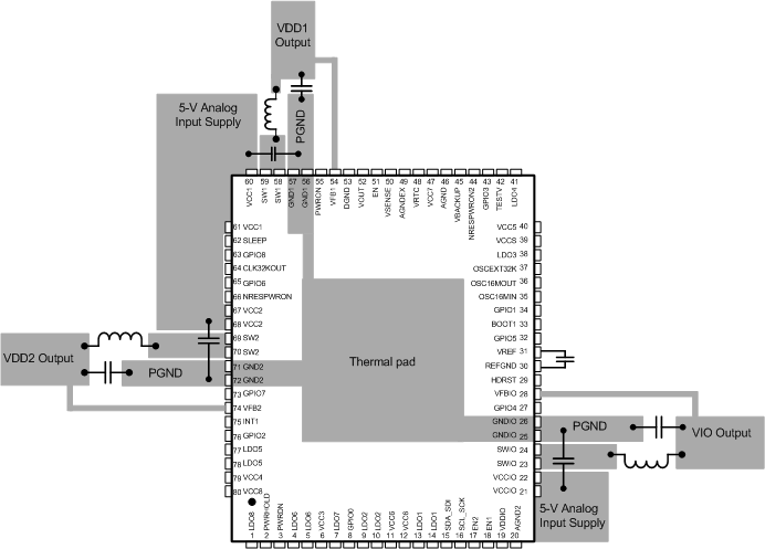
TPS659119-Q1 layout_swcs106.gif Figure 32. TPS659119-Q1 Layout Example