SLVSFN7 September 2020 TPS65982DMC
PRODUCTION DATA
- 1 Features
- 2 Applications
- 3 Description
- 4 Revision History
- 5 Pin Configuration and Functions
-
6 Specifications
- 6.1 Absolute Maximum Ratings
- 6.2 ESD Ratings
- 6.3 Recommended Operating Conditions
- 6.4 Thermal Information
- 6.5 Power Supply Requirements and Characteristics
- 6.6 Power Supervisor Characteristics
- 6.7 Adapter Power Switch Characteristics
- 6.8 USB Endpoint Requirements and Characteristics
- 6.9 Analog-to-Digital Converter (ADC) Characteristics
- 6.10 Input/Output (I/O) Requirements and Characteristics
- 6.11 I2C Slave Requirements and Characteristics
- 6.12 SPI Master Characteristics
- 6.13 Single-Wire Debugger (SWD) Timing Requirements
- 6.14 ADP_POWER_CFG Configuration Requirements
- 6.15 Thermal Shutdown Characteristics
- 6.16 Oscillator Requirements and Characteristics
- 7 Parameter Measurement Information
-
8 Detailed Description
- 8.1 Overview
- 8.2 Functional Block Diagram
- 8.3
Feature Description
- 8.3.1 Adapter Power Switch
- 8.3.2 USB Type-C Port Data Multiplexer
- 8.3.3 Power Management
- 8.3.4 Digital Core
- 8.3.5 System Glue Logic
- 8.3.6 Power Reset Congrol Module (PRCM)
- 8.3.7 Interrupt Monitor
- 8.3.8 ADC Sense
- 8.3.9 I2C Slave
- 8.3.10 SPI Master
- 8.3.11 Single-Wire Debugger Interface
- 8.3.12 ADC
- 8.3.13 I/O Buffers
- 8.3.14 Thermal Shutdown
- 8.3.15 Oscillators
- 8.4 Device Functional Modes
- 8.5 Programming
- 9 Application and Implementation
- 10Power Supply Recommendations
- 11Layout
- 12Device and Documentation Support
- 13Mechanical, Packaging, and Orderable Information
Package Options
Mechanical Data (Package|Pins)
- ZBH|96
Thermal pad, mechanical data (Package|Pins)
Orderable Information
8.3.2.1 USB2.0 Low-Speed Endpoint
The USB low-speed Endpoint is a USB 2.0 low-speed (1.5 Mbps) interface used to support HID class based accesses. The TPS65982DMC supports control of endpoint EP0. This endpoint enumerates to a USB 2.0 bus to provide USB-Billboard information to a host system as defined in the USB Type-C standard. EP0 is used for advertising the Billboard Class. When a host is connected to a device that provides Alternate Modes which cannot be supported by the host, the Billboard class allows a means for the host to report back to the user without any silent failures.
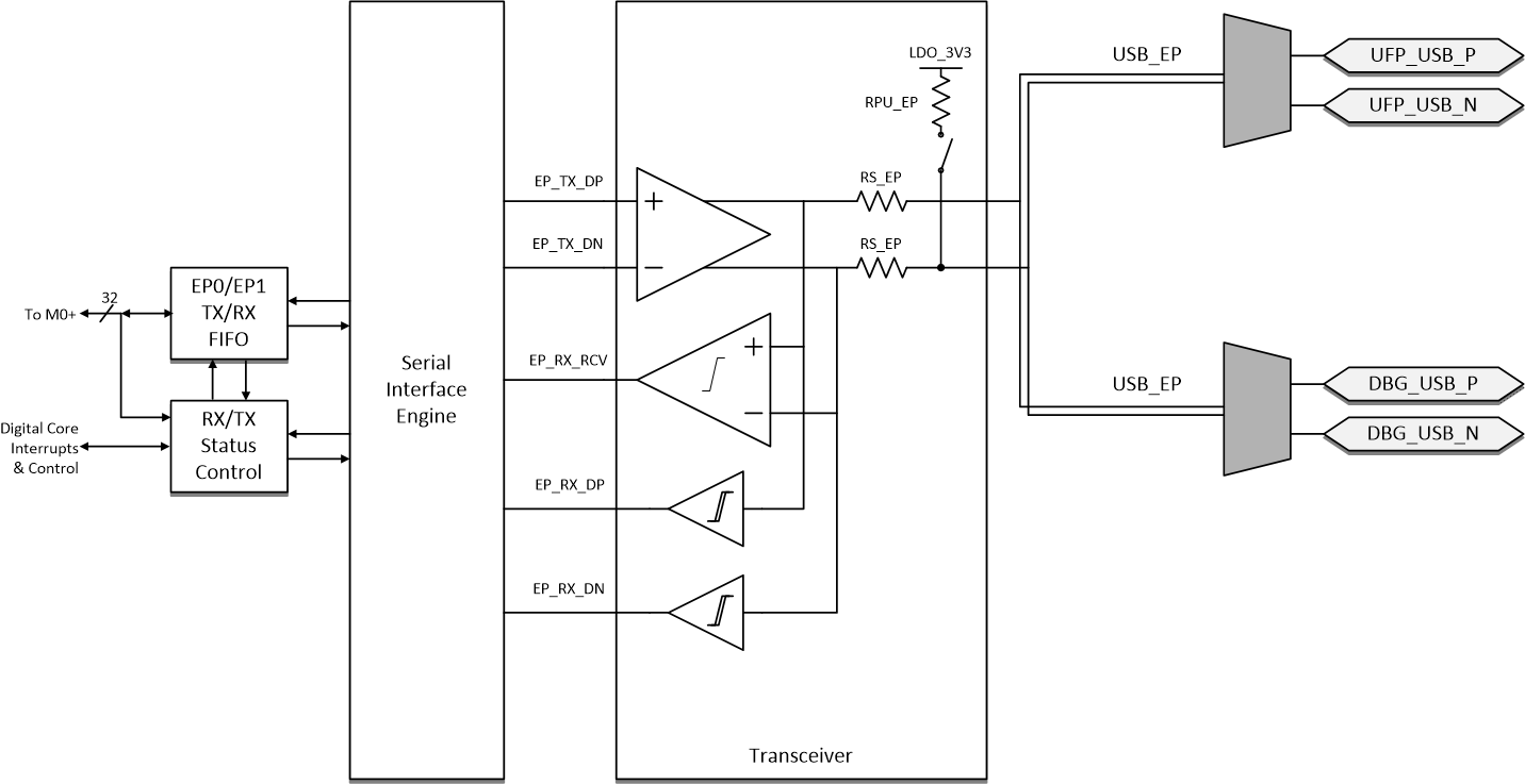
Figure 8-6 shows the USB Endpoint physical layer. The physical layer consists of the analog transceiver, the Serial Interface Engine, and the Endpoint FIFOs and supports low speed operation.
 Figure 8-6 USB Endpoint
Phy
Figure 8-6 USB Endpoint
PhyThe transceiver is made up of a fully differential output driver, a differential to single-ended receive buffer and two single-ended receive buffers on the D+/D– independently. The output driver drives the D+/D– of the selected output of the Port Multiplexer. The signals pass through the 2nd Stage Port Data Multiplexer to the port pins. When driving, the signal is driven through a source resistance RS_EP. RS_EP is shown as a single resistor in USB Endpoint Phy but this resistance also includes the resistance of the 2nd Stage Port Data Multiplexer defined in Port Data Multiplexer Requirements and Characteristics. RPU_EP is disconnected during transmit mode of the transceiver.
When the endpoint is in receive mode, the resistance RPU_EP is connected to the D– pin of the top or bottom port (UFP_USB_N or DBG_USB_N) depending on the operating condition. The RPU_EP resistance advertises low speed mode only.