SLVSFN7 September 2020 TPS65982DMC
PRODUCTION DATA
- 1 Features
- 2 Applications
- 3 Description
- 4 Revision History
- 5 Pin Configuration and Functions
-
6 Specifications
- 6.1 Absolute Maximum Ratings
- 6.2 ESD Ratings
- 6.3 Recommended Operating Conditions
- 6.4 Thermal Information
- 6.5 Power Supply Requirements and Characteristics
- 6.6 Power Supervisor Characteristics
- 6.7 Adapter Power Switch Characteristics
- 6.8 USB Endpoint Requirements and Characteristics
- 6.9 Analog-to-Digital Converter (ADC) Characteristics
- 6.10 Input/Output (I/O) Requirements and Characteristics
- 6.11 I2C Slave Requirements and Characteristics
- 6.12 SPI Master Characteristics
- 6.13 Single-Wire Debugger (SWD) Timing Requirements
- 6.14 ADP_POWER_CFG Configuration Requirements
- 6.15 Thermal Shutdown Characteristics
- 6.16 Oscillator Requirements and Characteristics
- 7 Parameter Measurement Information
-
8 Detailed Description
- 8.1 Overview
- 8.2 Functional Block Diagram
- 8.3
Feature Description
- 8.3.1 Adapter Power Switch
- 8.3.2 USB Type-C Port Data Multiplexer
- 8.3.3 Power Management
- 8.3.4 Digital Core
- 8.3.5 System Glue Logic
- 8.3.6 Power Reset Congrol Module (PRCM)
- 8.3.7 Interrupt Monitor
- 8.3.8 ADC Sense
- 8.3.9 I2C Slave
- 8.3.10 SPI Master
- 8.3.11 Single-Wire Debugger Interface
- 8.3.12 ADC
- 8.3.13 I/O Buffers
- 8.3.14 Thermal Shutdown
- 8.3.15 Oscillators
- 8.4 Device Functional Modes
- 8.5 Programming
- 9 Application and Implementation
- 10Power Supply Recommendations
- 11Layout
- 12Device and Documentation Support
- 13Mechanical, Packaging, and Orderable Information
Package Options
Mechanical Data (Package|Pins)
- ZBH|96
Thermal pad, mechanical data (Package|Pins)
Orderable Information
8.5.2.5 I2C Pin Address Setting
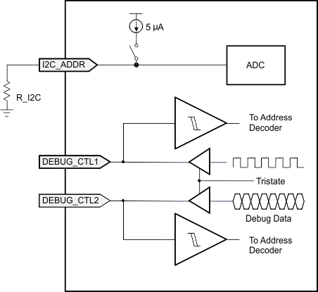
To enable the setting of multiple I2C addresses using a single TPS65982DMC pin, a resistance is placed externally on the I2C_ADDR pin. The internal ADC then decodes the address from this resistance value. Figure 8-27 shows the decoding. DEBUG_CTL1/2 are checked at the same time for the DC condition on this pin (high or low) for setting other bits of the address described previously. Note, DEBUG_CTL1/2 are GPIO and the address decoding is done by firmware in the digital core.
 Figure 8-27 I2C Address Decode
Table 8-5 lists the external resistance needed to set bits [3:1] of the I2C Unique Address. For the master TPS65982DMC, the pin is grounded.
Table 8-5 I2C Address Resistance
| TPS65982DMC DEVICE | EXTERNAL RESISTANCE (1%) | I2C UNIQUE ADDRESS [3:1] |
|---|---|---|
| Master 0 | 0 | 0x00 |
| Slave 7 | 38.3 k | 0x01 |
| Slave 6 | 84.5 k | 0x02 |
| Slave 5 | 140 k | 0x03 |
| Slave 4 | 205 k | 0x04 |
| Slave 3 | 280 k | 0x05 |
| Slave 2 | 374 k | 0x06 |
| Slave 1 | Open | 0x0F |