SLVSFN7 September 2020 TPS65982DMC
PRODUCTION DATA
- 1 Features
- 2 Applications
- 3 Description
- 4 Revision History
- 5 Pin Configuration and Functions
-
6 Specifications
- 6.1 Absolute Maximum Ratings
- 6.2 ESD Ratings
- 6.3 Recommended Operating Conditions
- 6.4 Thermal Information
- 6.5 Power Supply Requirements and Characteristics
- 6.6 Power Supervisor Characteristics
- 6.7 Adapter Power Switch Characteristics
- 6.8 USB Endpoint Requirements and Characteristics
- 6.9 Analog-to-Digital Converter (ADC) Characteristics
- 6.10 Input/Output (I/O) Requirements and Characteristics
- 6.11 I2C Slave Requirements and Characteristics
- 6.12 SPI Master Characteristics
- 6.13 Single-Wire Debugger (SWD) Timing Requirements
- 6.14 ADP_POWER_CFG Configuration Requirements
- 6.15 Thermal Shutdown Characteristics
- 6.16 Oscillator Requirements and Characteristics
- 7 Parameter Measurement Information
-
8 Detailed Description
- 8.1 Overview
- 8.2 Functional Block Diagram
- 8.3
Feature Description
- 8.3.1 Adapter Power Switch
- 8.3.2 USB Type-C Port Data Multiplexer
- 8.3.3 Power Management
- 8.3.4 Digital Core
- 8.3.5 System Glue Logic
- 8.3.6 Power Reset Congrol Module (PRCM)
- 8.3.7 Interrupt Monitor
- 8.3.8 ADC Sense
- 8.3.9 I2C Slave
- 8.3.10 SPI Master
- 8.3.11 Single-Wire Debugger Interface
- 8.3.12 ADC
- 8.3.13 I/O Buffers
- 8.3.14 Thermal Shutdown
- 8.3.15 Oscillators
- 8.4 Device Functional Modes
- 8.5 Programming
- 9 Application and Implementation
- 10Power Supply Recommendations
- 11Layout
- 12Device and Documentation Support
- 13Mechanical, Packaging, and Orderable Information
Package Options
Mechanical Data (Package|Pins)
- ZBH|96
Thermal pad, mechanical data (Package|Pins)
Orderable Information
8.3.13.1 IOBUF_GPIOLS and IOBUF_GPIOLSI2C
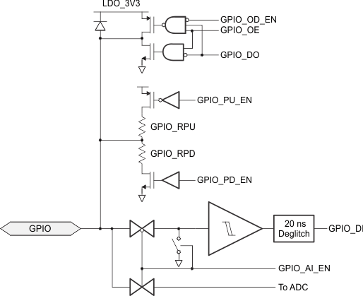
Figure 8-10 shows the GPIO I/O buffer for all GPIOn pins listed GPIO0-GPIO17 in Pin Functions. GPIOn pins can be mapped to application-specific events to control other ICs, interrupt a host processor, or receive input from another IC. This buffer is configurable to be a push-pull output, a weak push-pull, or open drain output. When configured as an input, the signal can be a deglitched digital input or an analog input to the ADC. The push-pull output is a simple CMOS output with independent pulldown control allowing open-drain connections. The weak push-pull is also a CMOS output, but with GPIO_RPU resistance in series with the drain. The supply voltage to this buffer is configurable to be LDO_3V3 by default or VDDIO. For simplicity, the connection to VDDIO is not shown in Figure 8-10, but the connection to VDDIO is fail-safe and a diode will not be present from GPIOn to VDDIO in this configuration. The pullup and pulldown output drivers are independently controlled from the input and are enabled or disabled via application code in the digital core.
 Figure 8-10 IOBUF_GPIOLS (General GPIO) I/O
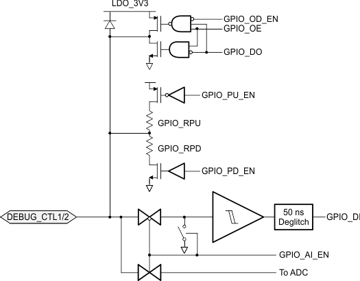
Figure 8-11 shows the IOBUF_GPIOLSI2C that is identical to IOBUF_GPIOLS with an extended deglitch time.
 Figure 8-11 IOBUF_GPIOLSI2C (General GPIO) I/O with I2C Deglitch