SLVSFN7 September 2020 TPS65982DMC
PRODUCTION DATA
- 1 Features
- 2 Applications
- 3 Description
- 4 Revision History
- 5 Pin Configuration and Functions
-
6 Specifications
- 6.1 Absolute Maximum Ratings
- 6.2 ESD Ratings
- 6.3 Recommended Operating Conditions
- 6.4 Thermal Information
- 6.5 Power Supply Requirements and Characteristics
- 6.6 Power Supervisor Characteristics
- 6.7 Adapter Power Switch Characteristics
- 6.8 USB Endpoint Requirements and Characteristics
- 6.9 Analog-to-Digital Converter (ADC) Characteristics
- 6.10 Input/Output (I/O) Requirements and Characteristics
- 6.11 I2C Slave Requirements and Characteristics
- 6.12 SPI Master Characteristics
- 6.13 Single-Wire Debugger (SWD) Timing Requirements
- 6.14 ADP_POWER_CFG Configuration Requirements
- 6.15 Thermal Shutdown Characteristics
- 6.16 Oscillator Requirements and Characteristics
- 7 Parameter Measurement Information
-
8 Detailed Description
- 8.1 Overview
- 8.2 Functional Block Diagram
- 8.3
Feature Description
- 8.3.1 Adapter Power Switch
- 8.3.2 USB Type-C Port Data Multiplexer
- 8.3.3 Power Management
- 8.3.4 Digital Core
- 8.3.5 System Glue Logic
- 8.3.6 Power Reset Congrol Module (PRCM)
- 8.3.7 Interrupt Monitor
- 8.3.8 ADC Sense
- 8.3.9 I2C Slave
- 8.3.10 SPI Master
- 8.3.11 Single-Wire Debugger Interface
- 8.3.12 ADC
- 8.3.13 I/O Buffers
- 8.3.14 Thermal Shutdown
- 8.3.15 Oscillators
- 8.4 Device Functional Modes
- 8.5 Programming
- 9 Application and Implementation
- 10Power Supply Recommendations
- 11Layout
- 12Device and Documentation Support
- 13Mechanical, Packaging, and Orderable Information
Package Options
Mechanical Data (Package|Pins)
- ZBH|96
Thermal pad, mechanical data (Package|Pins)
Orderable Information
8.4.1 Boot Code
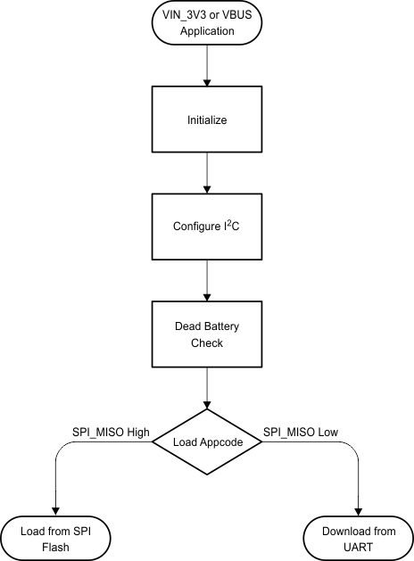
The TPS65982DMC has a Power-on-Reset (POR) circuit that monitors LDO_3V3 and issues an internal reset signal. The digital core, memory banks, and peripherals receive clock and RESET interrupt is issued to the digital core and the boot code starts executing. Figure 8-16 provides the TPS65982DMC boot code sequence.
The TPS65982DMC boot code is loaded from OTP on POR, and begins initializing TPS65982DMC settings. This initialization includes enabling and resetting internal registers, loading trim values, waiting for the trim values to settle, and configuring the device I2C addresses.
The unique I2C address is based on the customer programmable OTP, DEBUG_CTLX pins, and resistor configuration on the I2C_ADDR pin.
Once initial device configuration is complete the boot code determines if the TPS65982DMC is booting under dead battery condition (VIN_3V3 invalid, ADP_IN valid). If the boot code determines the TPS65982DMC is booting under dead battery condition, the ADP_POWER_CFG pin is sampled to determine if the adapter power switch from ADP_IN should be enabled.
 Figure 8-16 Flow Diagram for Boot Code Sequence