SLVSES1D May   2018  – October 2022 TPS65987D

PRODUCTION DATA  

  1. Features
  2. Applications
  3. Description
  4. Revision History
  5. Pin Configuration and Functions
  6. Specifications
    1. 6.1  Absolute Maximum Ratings
    2. 6.2  ESD Ratings
    3. 6.3  Recommended Operating Conditions
    4. 6.4  Thermal Information
    5. 6.5  Power Supply Requirements and Characteristics
    6. 6.6  Power Consumption Characteristics
    7. 6.7  Power Switch Characteristics
    8. 6.8  Cable Detection Characteristics
    9. 6.9  USB-PD Baseband Signal Requirements and Characteristics
    10. 6.10 BC1.2 Characteristics
    11. 6.11 Thermal Shutdown Characteristics
    12. 6.12 Oscillator Characteristics
    13. 6.13 I/O Characteristics
    14. 6.14 PWM Driver Characteristics
    15. 6.15 I2C Requirements and Characteristics
    16. 6.16 SPI Controller Timing Requirements
    17. 6.17 HPD Timing Requirements
    18. 6.18 Typical Characteristics
  7. Parameter Measurement Information
  8. Detailed Description
    1. 8.1 Overview
    2. 8.2 Functional Block Diagram
    3. 8.3 Feature Description
      1. 8.3.1  USB-PD Physical Layer
        1. 8.3.1.1 USB-PD Encoding and Signaling
        2. 8.3.1.2 USB-PD Bi-Phase Marked Coding
        3. 8.3.1.3 USB-PD Transmit (TX) and Receive (Rx) Masks
        4. 8.3.1.4 USB-PD BMC Transmitter
        5. 8.3.1.5 USB-PD BMC Receiver
      2. 8.3.2  Power Management
        1. 8.3.2.1 Power-On And Supervisory Functions
        2. 8.3.2.2 VBUS LDO
        3. 8.3.2.3 Supply Switch Over
      3. 8.3.3  Port Power Switches
        1. 8.3.3.1 PP_HV Power Switch
          1. 8.3.3.1.1 PP_HV Over Current Clamp
          2. 8.3.3.1.2 PP_HV Over Current Protection
          3. 8.3.3.1.3 PP_HV OVP and UVP
          4. 8.3.3.1.4 PP_HV Reverse Current Protection
        2. 8.3.3.2 Schottky for Current Surge Protection
        3. 8.3.3.3 PP_EXT Power Path Control
        4. 8.3.3.4 PP_CABLE Power Switch
          1. 8.3.3.4.1 PP_CABLE Over Current Protection
          2. 8.3.3.4.2 PP_CABLE Input Good Monitor
        5. 8.3.3.5 VBUS Transition to VSAFE5V
        6. 8.3.3.6 VBUS Transition to VSAFE0V
      4. 8.3.4  Cable Plug and Orientation Detection
        1. 8.3.4.1 Configured as a DFP
        2. 8.3.4.2 Configured as a UFP
        3. 8.3.4.3 Configured as a DRP
        4. 8.3.4.4 Fast Role Swap Signaling
      5. 8.3.5  Dead Battery Operation
        1. 8.3.5.1 Dead Battery Advertisement
        2. 8.3.5.2 BUSPOWER (ADCIN1)
      6. 8.3.6  Battery Charger Detection and Advertisement
        1. 8.3.6.1 BC1.2 Data Contact Detect
        2. 8.3.6.2 BC1.2 Primary and Secondary Detection
        3. 8.3.6.3 Charging Downstream Port Advertisement
        4. 8.3.6.4 Dedicated Charging Port Advertisement
        5. 8.3.6.5 2.7V Divider3 Mode Advertisement
        6. 8.3.6.6 1.2V Mode Advertisement
        7. 8.3.6.7 DCP Auto Mode Advertisement
      7. 8.3.7  ADC
      8. 8.3.8  DisplayPort HPD
      9. 8.3.9  Digital Interfaces
        1. 8.3.9.1 General GPIO
        2. 8.3.9.2 I2C
        3. 8.3.9.3 SPI
      10. 8.3.10 PWM Driver
      11. 8.3.11 Digital Core
      12. 8.3.12 I2C Interfaces
        1. 8.3.12.1 I2C Interface Description
        2. 8.3.12.2 I2C Clock Stretching
        3. 8.3.12.3 I2C Address Setting
        4. 8.3.12.4 Unique Address Interface
        5. 8.3.12.5 I2C Pin Address Setting (ADCIN2)
      13. 8.3.13 SPI Controller Interface
      14. 8.3.14 Thermal Shutdown
      15. 8.3.15 Oscillators
    4. 8.4 Device Functional Modes
      1. 8.4.1 Boot
      2. 8.4.2 Power States
  9. Application and Implementation
    1. 9.1 Application Information
    2. 9.2 Typical Application
      1. 9.2.1 Type-C VBUS Design Considerations
        1. 9.2.1.1 Design Requirements
        2. 9.2.1.2 Detailed Design Procedure
          1. 9.2.1.2.1 Type-C Connector VBUS Capacitors
          2. 9.2.1.2.2 VBUS Schottky and TVS Diodes
          3. 9.2.1.2.3 VBUS Snubber Circuit
        3. 9.2.1.3 Application Curves
      2. 9.2.2 Notebook Design Supporting PD Charging
        1. 9.2.2.1 USB and DisplayPort Notebook Supporting PD Charging
          1. 9.2.2.1.1 Design Requirements
          2. 9.2.2.1.2 Detailed Design Procedure
            1. 9.2.2.1.2.1 USB Power Delivery Source Capabilities
            2. 9.2.2.1.2.2 USB Power Delivery Sink Capabilities
            3. 9.2.2.1.2.3 USB and DisplayPort Supported Data Modes
            4. 9.2.2.1.2.4 TUSB1046 Super Speed Mux GPIO Control
        2. 9.2.2.2 Thunderbolt Notebook Supporting PD Charging
          1. 9.2.2.2.1 Design Requirements
          2. 9.2.2.2.2 Detailed Design Procedure
            1. 9.2.2.2.2.1 USB Power Delivery Source Capabilities
            2. 9.2.2.2.2.2 USB Power Delivery Sink Capabilities
            3. 9.2.2.2.2.3 Thunderbolt Supported Data Modes
            4. 9.2.2.2.2.4 RESETN
            5. 9.2.2.2.2.5 I2C Design Requirements
            6. 9.2.2.2.2.6 TS3DS10224 SBU Mux for AUX and LSTX/RX
            7. 9.2.2.2.2.7 Thunderbolt Flash Options
        3. 9.2.2.3 USB and DisplayPort Dock with Bus-Powered and Self-Powered Support
          1. 9.2.2.3.1 Design Requirements
          2. 9.2.2.3.2 Detailed Design Procedure
            1. 9.2.2.3.2.1 USB Power Delivery Source Capabilities
            2. 9.2.2.3.2.2 USB Power Delivery Sink Capabilities
            3. 9.2.2.3.2.3 USB and DisplayPort Supported Data Modes
            4. 9.2.2.3.2.4 TUSB1064 Super Speed Mux GPIO Control
  10. 10Power Supply Recommendations
    1. 10.1 3.3-V Power
      1. 10.1.1 VIN_3V3 Input Switch
      2. 10.1.2 VBUS 3.3-V LDO
    2. 10.2 1.8-V Power
    3. 10.3 Recommended Supply Load Capacitance
  11. 11Layout
    1. 11.1 Layout Guidelines
      1. 11.1.1 Top TPS65987D Placement and Bottom Component Placement and Layout
    2. 11.2 Layout Example
    3. 11.3 Component Placement
    4. 11.4 Routing PP_HV1/2, VBUS, PP_CABLE, VIN_3V3, LDO_3V3, LDO_1V8
    5. 11.5 Routing CC and GPIO
    6. 11.6 Thermal Dissipation for FET Drain Pads
    7. 11.7 USB2 Recommended Routing For BC1.2 Detection/Advertisement
  12. 12Device and Documentation Support
    1. 12.1 Device Support
      1. 12.1.1 Third-Party Products Disclaimer
      2. 12.1.2 Firmware Warranty Disclaimer
    2. 12.2 Receiving Notification of Documentation Updates
    3. 12.3 Support Resources
    4. 12.4 Trademarks
    5. 12.5 Electrostatic Discharge Caution
    6. 12.6 Glossary
  13. 13Mechanical, Packaging, and Orderable Information

Package Options

Mechanical Data (Package|Pins)
Thermal pad, mechanical data (Package|Pins)
Orderable Information

USB and DisplayPort Notebook Supporting PD Charging

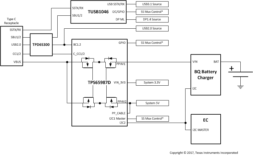
For systems that support USB and DisplayPort Data, the USB and DisplayPort sources are muxed to the Type-C connector through the TUSB1046 Super Speed mux. The TPS65987D is capable of controlling the Super Speed Mux over I2C and will configure it according to the connection at the Type-C connector. The TPS65987D can also set the configurations for the Super Speed mux equalizer settings for the USB Super Speed and DisplayPort Lanes through an initializing set of I2C writes. Note that I2C1 is the I2C master controlling the SS Mux and I2C2 is connected to the embedded controller. I2C1 can operate as an I2C master/slave and I2C2 can only operate as an I2C slave. Alternatively the Super Speed mux can be controlled through GPIO instead of I2C. The TPD6S300 provides Type-C protection features such as short to VBUS on the CC and SBU pins and ESD protection for the USB2 DN/P. See the figure below for the system block diagram.
GUID-B96C85AE-6FD4-4F65-B094-737C89D72657-low.gif Figure 9-6 USB and DisplayPort Notebook Supporting PD Charging