SLVSF34B May   2019  – October 2022 TPS65987DDJ

PRODUCTION DATA  

  1. Features
  2. Applications
  3. Description
  4. Revision History
  5. Pin Configuration and Functions
  6. Specifications
    1. 6.1  Absolute Maximum Ratings
    2. 6.2  ESD Ratings
    3. 6.3  Recommended Operating Conditions
    4. 6.4  Thermal Information
    5. 6.5  Power Supply Requirements and Characteristics
    6. 6.6  Power Consumption Characteristics
    7. 6.7  Power Switch Characteristics
    8. 6.8  Cable Detection Characteristics
    9. 6.9  USB-PD Baseband Signal Requirements and Characteristics
    10. 6.10 BC1.2 Characteristics
    11. 6.11 Thermal Shutdown Characteristics
    12. 6.12 Oscillator Characteristics
    13. 6.13 I/O Characteristics
    14. 6.14 I2C Requirements and Characteristics
    15. 6.15 SPI Controller Timing Requirements
    16. 6.16 HPD Timing Requirements
    17. 6.17 Typical Characteristics
  7. Parameter Measurement Information
  8. Detailed Description
    1. 8.1 Overview
    2. 8.2 Functional Block Diagram
    3. 8.3 Feature Description
      1. 8.3.1  USB-PD Physical Layer
        1. 8.3.1.1 USB-PD Encoding and Signaling
        2. 8.3.1.2 USB-PD Bi-Phase Marked Coding
        3. 8.3.1.3 USB-PD Transmit (TX) and Receive (Rx) Masks
        4. 8.3.1.4 USB-PD BMC Transmitter
        5. 8.3.1.5 USB-PD BMC Receiver
      2. 8.3.2  Power Management
        1. 8.3.2.1 Power-On And Supervisory Functions
        2. 8.3.2.2 VBUS LDO
        3. 8.3.2.3 Supply Switch Over
      3. 8.3.3  Port Power Switches
        1. 8.3.3.1 PP_HV Power Switch
          1. 8.3.3.1.1 PP_HV Overcurrent Clamp
          2. 8.3.3.1.2 PP_HV Overcurrent Protection
          3. 8.3.3.1.3 PP_HV OVP and UVP
          4. 8.3.3.1.4 PP_HV Reverse Current Protection
        2. 8.3.3.2 Schottky for Current Surge Protection
        3. 8.3.3.3 PP_EXT Power Path Control
        4. 8.3.3.4 PP_CABLE Power Switch
          1. 8.3.3.4.1 PP_CABLE Overcurrent Protection
          2. 8.3.3.4.2 PP_CABLE Input Good Monitor
        5. 8.3.3.5 VBUS Transition to VSAFE5V
        6. 8.3.3.6 VBUS Transition to VSAFE0V
      4. 8.3.4  Cable Plug and Orientation Detection
        1. 8.3.4.1 Configured as a DFP
        2. 8.3.4.2 Configured as a UFP
        3. 8.3.4.3 Configured as a DRP
        4. 8.3.4.4 Fast Role Swap Signaling
      5. 8.3.5  Dead Battery Operation
        1. 8.3.5.1 Dead Battery Advertisement
        2. 8.3.5.2 BUSPOWER (ADCIN1)
      6. 8.3.6  Battery Charger Detection and Advertisement
        1. 8.3.6.1 BC1.2 Data Contact Detect
        2. 8.3.6.2 BC1.2 Primary and Secondary Detection
        3. 8.3.6.3 Charging Downstream Port Advertisement
        4. 8.3.6.4 Dedicated Charging Port Advertisement
        5. 8.3.6.5 2.7-V Divider3 Mode Advertisement
        6. 8.3.6.6 1.2-V Mode Advertisement
        7. 8.3.6.7 DCP Auto Mode Advertisement
      7. 8.3.7  ADC
      8. 8.3.8  DisplayPort HPD
      9. 8.3.9  Digital Interfaces
        1. 8.3.9.1 General GPIO
        2. 8.3.9.2 I2C
        3. 8.3.9.3 SPI
      10. 8.3.10 Digital Core
      11. 8.3.11 I2C Interfaces
        1. 8.3.11.1 I2C Interface Description
        2. 8.3.11.2 I2C Clock Stretching
        3. 8.3.11.3 I2C Address Setting
        4. 8.3.11.4 Unique Address Interface
        5. 8.3.11.5 I2C Pin Address Setting (ADCIN2)
      12. 8.3.12 SPI Controller Interface
      13. 8.3.13 Thermal Shutdown
      14. 8.3.14 Oscillators
    4. 8.4 Device Functional Modes
      1. 8.4.1 Boot
      2. 8.4.2 Power States
  9. Application and Implementation
    1. 9.1 Application Information
    2. 9.2 Typical Applications
      1. 9.2.1 Type-C VBUS Design Considerations
        1. 9.2.1.1 Design Requirements
        2. 9.2.1.2 Detailed Design Procedure
          1. 9.2.1.2.1 Type-C Connector VBUS Capacitors
          2. 9.2.1.2.2 VBUS Schottky and TVS Diodes
          3. 9.2.1.2.3 VBUS Snubber Circuit
        3. 9.2.1.3 Application Curves
      2. 9.2.2 Notebook Design Supporting PD Charging
        1. 9.2.2.1 USB and DisplayPort Notebook Supporting PD Charging
          1. 9.2.2.1.1 Design Requirements
          2. 9.2.2.1.2 Detailed Design Procedure
            1. 9.2.2.1.2.1 USB Power Delivery Source Capabilities
            2. 9.2.2.1.2.2 USB Power Delivery Sink Capabilities
            3. 9.2.2.1.2.3 f
            4. 9.2.2.1.2.4 TUSB1046 Super Speed Mux GPIO Control
        2. 9.2.2.2 Thunderbolt Notebook Supporting PD Charging
          1. 9.2.2.2.1 Design Requirements
          2. 9.2.2.2.2 Detailed Design Procedure
            1. 9.2.2.2.2.1 USB Power Delivery Source Capabilities
            2. 9.2.2.2.2.2 USB Power Delivery Sink Capabilities
            3. 9.2.2.2.2.3 Thunderbolt Supported Data Modes
            4. 9.2.2.2.2.4 RESETN
            5. 9.2.2.2.2.5 I2C Design Requirements
            6. 9.2.2.2.2.6 TS3DS10224 SBU Mux for AUX and LSTX/RX
            7. 9.2.2.2.2.7 Thunderbolt Flash Options
        3. 9.2.2.3 USB and DisplayPort Dock with Bus-Powered and Self-Powered Support
          1. 9.2.2.3.1 Design Requirements
          2. 9.2.2.3.2 Detailed Design Procedure
            1. 9.2.2.3.2.1 USB Power Delivery Source Capabilities
            2. 9.2.2.3.2.2 USB Power Delivery Sink Capabilities
            3. 9.2.2.3.2.3 USB and DisplayPort Supported Data Modes
            4. 9.2.2.3.2.4 TUSB1064 Super Speed Mux GPIO Control
  10. 10Power Supply Recommendations
    1. 10.1 3.3-V Power
      1. 10.1.1 VIN_3V3 Input Switch
      2. 10.1.2 VBUS 3.3-V LDO
    2. 10.2 1.8-V Power
    3. 10.3 Recommended Supply Load Capacitance
  11. 11Layout
    1. 11.1 Layout Guidelines
      1. 11.1.1 Top TPS65987DDJ Placement and Bottom Component Placement and Layout
    2. 11.2 Layout Example
    3. 11.3 Component Placement
    4. 11.4 Routing PP_HV1/2, VBUS, PP_CABLE, VIN_3V3, LDO_3V3, LDO_1V8
    5. 11.5 Routing CC and GPIO
    6. 11.6 Thermal Dissipation for FET Drain Pads
    7. 11.7 USB2 Recommended Routing For BC1.2 Detection/Advertisement
  12. 12Device and Documentation Support
    1. 12.1 Device Support
      1. 12.1.1 Third-Party Products Disclaimer
      2. 12.1.2 Firmware Warranty Disclaimer
    2. 12.2 Documentation Support
      1. 12.2.1 Related Documentation
    3. 12.3 Receiving Notification of Documentation Updates
    4. 12.4 Support Resources
    5. 12.5 Trademarks
    6. 12.6 Electrostatic Discharge Caution
    7. 12.7 Glossary
  13. 13Mechanical, Packaging, and Orderable Information

Package Options

Mechanical Data (Package|Pins)
Thermal pad, mechanical data (Package|Pins)
Orderable Information
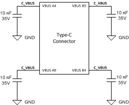
Type-C Connector VBUS Capacitors
GUID-2C5A7D6D-FF3A-4EB4-8F21-61CD2FA0779F-low.gifFigure 9-2 Type-C Connector VBUS Capacitors

The first level of protection starts at the Type-C connector and the VBUS pin capacitors. These capacitors help filter out high frequency noise but can also help absorb short voltage transients. Each VBUS pin should have a 10-nF capacitor rated at or above 25 V and placed as close to the pin as possible. The GND pin on the capacitors should have very short path to GND on the connector. The derating factor of ceramic capacitors should be taken into account as they can lose more than 50% of their effective capacitance when biased. Adding the VBUS capacitors can help reduce voltage spikes by 2 V to 3 V.