SLVSDB5B July   2018  – August 2021 TPS65988

PRODUCTION DATA  

  1. Features
  2. Applications
  3. Description
  4. Revision History
  5. Pin Configuration and Functions
  6. Specifications
    1. 6.1  Absolute Maximum Ratings
    2. 6.2  ESD Ratings
    3. 6.3  Recommended Operating Conditions
    4. 6.4  Thermal Information
    5. 6.5  Power Supply Requirements and Characteristics
    6. 6.6  Power Consumption Characteristics
    7. 6.7  Power Switch Characteristics
    8. 6.8  Cable Detection Characteristics
    9. 6.9  USB-PD Baseband Signal Requirements and Characteristics
    10. 6.10 BC1.2 Characteristics
    11. 6.11 Thermal Shutdown Characteristics
    12. 6.12 Oscillator Characteristics
    13. 6.13 I/O Characteristics
    14. 6.14 PWM Driver Characteristics
    15. 6.15 I2C Requirements and Characteristics
    16. 6.16 SPI Controller Timing Requirements
    17. 6.17 HPD Timing Requirements
    18. 6.18 Typical Characteristics
  7. Parameter Measurement Information
  8. Detailed Description
    1. 8.1 Overview
    2. 8.2 Functional Block Diagram
    3. 8.3 Feature Description
      1. 8.3.1  USB-PD Physical Layer
        1. 8.3.1.1 USB-PD Encoding and Signaling
        2. 8.3.1.2 USB-PD Bi-Phase Marked Coding
        3. 8.3.1.3 USB-PD Transmit (TX) and Receive (Rx) Masks
        4. 8.3.1.4 USB-PD BMC Transmitter
        5. 8.3.1.5 USB-PD BMC Receiver
      2. 8.3.2  Power Management
        1. 8.3.2.1 Power-On And Supervisory Functions
        2. 8.3.2.2 VBUS LDO
        3. 8.3.2.3 Supply Switch Over
      3. 8.3.3  Port Power Switches
        1. 8.3.3.1 PP_HV Power Switch
          1. 8.3.3.1.1 PP_HV Over Current Clamp
          2. 8.3.3.1.2 PP_HV Over Current Protection
          3. 8.3.3.1.3 PP_HV OVP and UVP
          4. 8.3.3.1.4 PP_HV Reverse Current Protection
        2. 8.3.3.2 Schottky for Current Surge Protection
        3. 8.3.3.3 PP_EXT Power Path Control
        4. 8.3.3.4 PP_CABLE Power Switch
          1. 8.3.3.4.1 PP_CABLE Over Current Protection
          2. 8.3.3.4.2 PP_CABLE Input Good Monitor
        5. 8.3.3.5 VBUS Transition to VSAFE5V
        6. 8.3.3.6 VBUS Transition to VSAFE0V
      4. 8.3.4  Cable Plug and Orientation Detection
        1. 8.3.4.1 Configured as a DFP
        2. 8.3.4.2 Configured as a UFP
        3. 8.3.4.3 Configured as a DRP
        4. 8.3.4.4 Fast Role Swap Signaling
      5. 8.3.5  Dead Battery Operation
        1. 8.3.5.1 Dead Battery Advertisement
        2. 8.3.5.2 BUSPOWER (ADCIN1)
      6. 8.3.6  Battery Charger Detection and Advertisement
        1. 8.3.6.1 BC1.2 Data Contact Detect
        2. 8.3.6.2 BC1.2 Primary and Secondary Detection
        3. 8.3.6.3 Charging Downstream Port Advertisement
        4. 8.3.6.4 Dedicated Charging Port Advertisement
        5. 8.3.6.5 2.7V Divider3 Mode Advertisement
        6. 8.3.6.6 1.2V Mode Advertisement
        7. 8.3.6.7 DCP Auto Mode Advertisement
      7. 8.3.7  ADC
      8. 8.3.8  DisplayPort HPD
      9. 8.3.9  Digital Interfaces
        1. 8.3.9.1 General GPIO
        2. 8.3.9.2 I2C
        3. 8.3.9.3 SPI
      10. 8.3.10 PWM Driver
      11. 8.3.11 Digital Core
      12. 8.3.12 I2C Interfaces
        1. 8.3.12.1 I2C Interface Description
        2. 8.3.12.2 I2C Clock Stretching
        3. 8.3.12.3 I2C Address Setting
        4. 8.3.12.4 Unique Address Interface
        5. 8.3.12.5 I2C Pin Address Setting (ADCIN2)
      13. 8.3.13 SPI Controller Interface
      14. 8.3.14 Thermal Shutdown
      15. 8.3.15 Oscillators
    4. 8.4 Device Functional Modes
      1. 8.4.1 Boot
      2. 8.4.2 Power States
  9. Application and Implementation
    1. 9.1 Application Information
    2. 9.2 Typical Applications
      1. 9.2.1 Type-C VBUS Design Considerations
        1. 9.2.1.1 Design Requirements
        2. 9.2.1.2 Detailed Design Procedure
          1. 9.2.1.2.1 External Sink Power Path Options
            1. 9.2.1.2.1.1 Load Switch Power Path
            2. 9.2.1.2.1.2 Discrete Power Path
          2. 9.2.1.2.2 Type-C Connector VBUS Capacitors
          3. 9.2.1.2.3 VBUS Schottky and TVS Diodes
          4. 9.2.1.2.4 VBUS Snubber Circuit
        3. 9.2.1.3 Application Curves
      2. 9.2.2 Dual Port Thunderbolt Notebook with AR Supporting USB PD Charging
        1. 9.2.2.1 Design Requirements
        2. 9.2.2.2 USB Power Delivery Source Capabilities
        3. 9.2.2.3 USB Power Delivery Sink Capabilities
        4. 9.2.2.4 Supported Data Modes
        5. 9.2.2.5 RESETN
        6. 9.2.2.6 I2C Design Requirements
        7. 9.2.2.7 TS3DS10224 SBU Mux for AUX and LSTX/RX
        8. 9.2.2.8 Thunderbolt Flash Options
      3. 9.2.3 Dual Port USB & Displayport Notebook Supporting PD Charging
        1. 9.2.3.1 Design Requirements
        2. 9.2.3.2 USB Power Delivery Source Capabilities
        3. 9.2.3.3 USB Power Delivery Sink Capabilities
        4. 9.2.3.4 Supported Data Modes
        5. 9.2.3.5 TUSB1044 Re-Driver GPIO Control
      4. 9.2.4 USB Type-C & PD Monitor/Dock
        1. 9.2.4.1 Design Requirements
        2. 9.2.4.2 Detailed Design Procedure
          1. 9.2.4.2.1 USB Power Delivery Source Capabilities
          2. 9.2.4.2.2 USB and DisplayPort Supported Data Modes
          3. 9.2.4.2.3 TUSB1064 Super Speed Mux GPIO Control
  10. 10Power Supply Recommendations
    1. 10.1 3.3-V Power
      1. 10.1.1 VIN_3V3 Input Switch
      2. 10.1.2 VBUS 3.3-V LDO
    2. 10.2 1.8-V Power
    3. 10.3 Recommended Supply Load Capacitance
  11. 11Layout
    1. 11.1  Layout Guidelines
    2. 11.2  Layout Example
    3. 11.3  Stack-Up and Design Rules
    4. 11.4  Main Component Placement
    5. 11.5  1.4 Super Speed Type-C Connectors
    6. 11.6  Capacitor Placement
    7. 11.7  CC1/2 Capacitors & ADCIN1/2 Resistors
    8. 11.8  CC & SBU Protection Placement
    9. 11.9  CC Routing
    10. 11.10 DRAIN1 and DRAIN2 Pad Pours
    11. 11.11 USB2 Routing for ESD Protection and BC1.2
    12. 11.12 VBUS Routing
    13. 11.13 Completed Layout
    14. 11.14 Power Dissipation
  12. 12Device and Documentation Support
    1. 12.1 Device Support
      1. 12.1.1 Third-Party Products Disclaimer
      2. 12.1.2 Firmware Warranty Disclaimer
    2. 12.2 Receiving Notification of Documentation Updates
    3. 12.3 Support Resources
    4. 12.4 Trademarks
    5. 12.5 Electrostatic Discharge Caution
    6. 12.6 Glossary
  13. 13Mechanical, Packaging, and Orderable Information

Package Options

Mechanical Data (Package|Pins)
Thermal pad, mechanical data (Package|Pins)
Orderable Information

Dual Port USB & Displayport Notebook Supporting PD Charging

Certain SoCs can support USB and DisplayPort and the muxing required for Type-C. The systems that use this architecture may need a re-driver to ensure signal signal integrity to from the SoC to the Type-C connectors. Generally the SoC is controlled through I2C and must be connected to the I2C1 Master on the TPS65988. A re-driver can be controlled through GPIO or I2C. The Embedded controller is connected to the I2C2 Slave on the TPS65988. Figure 9-9 shows the SoC controlled though I2C and the Re-Driver controlled through GPIO. Figure 9-10 shows the SoC & Re-Driver controlled though I2C. The TPS65988’s two internal power paths provide VBUS which is taken from the System 5 V for Port and will control the external sink path to charge the system through USB PD. The System 5 V will also power PP_CABLE1/2 on the TPS65988 to supply VCONN to Type-C e-marked cables and Type-C accessories. An embedded controller EC is used to communicate to the TPS65988 for additional control and to relay information back to the operating system. An embedded controller can control additional features such as entering and exiting sleep modes, changing source and sink capabilities depending on the state of the battery, UCSI support, control alternate modes, etc. Refer to the Host Interface and Firmware users guide for additional information.
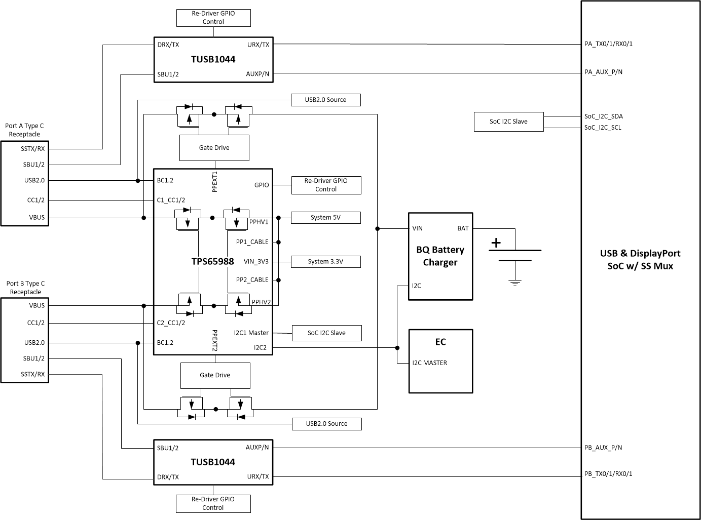
GUID-9D22B360-1FB1-4B87-AFE6-147295BA75C1-low.gifFigure 9-9 TPS65988 and SoC I2C with Re-Driver GPIO
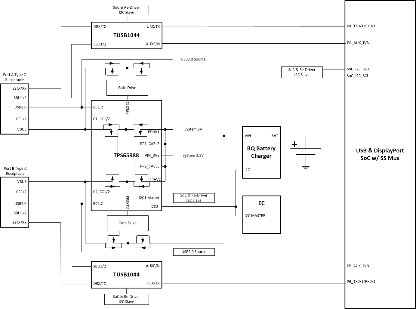
GUID-A3493C78-08E3-43EC-A0F6-D3AE4805FD8E-low.gifFigure 9-10 TPS65988 and SoC & Redriver I2C