SLVSDB5B July 2018 – August 2021 TPS65988
PRODUCTION DATA
- 1 Features
- 2 Applications
- 3 Description
- 4 Revision History
- 5 Pin Configuration and Functions
-
6 Specifications
- 6.1 Absolute Maximum Ratings
- 6.2 ESD Ratings
- 6.3 Recommended Operating Conditions
- 6.4 Thermal Information
- 6.5 Power Supply Requirements and Characteristics
- 6.6 Power Consumption Characteristics
- 6.7 Power Switch Characteristics
- 6.8 Cable Detection Characteristics
- 6.9 USB-PD Baseband Signal Requirements and Characteristics
- 6.10 BC1.2 Characteristics
- 6.11 Thermal Shutdown Characteristics
- 6.12 Oscillator Characteristics
- 6.13 I/O Characteristics
- 6.14 PWM Driver Characteristics
- 6.15 I2C Requirements and Characteristics
- 6.16 SPI Controller Timing Requirements
- 6.17 HPD Timing Requirements
- 6.18 Typical Characteristics
- 7 Parameter Measurement Information
-
8 Detailed Description
- 8.1 Overview
- 8.2 Functional Block Diagram
- 8.3
Feature Description
- 8.3.1 USB-PD Physical Layer
- 8.3.2 Power Management
- 8.3.3 Port Power Switches
- 8.3.4 Cable Plug and Orientation Detection
- 8.3.5 Dead Battery Operation
- 8.3.6 Battery Charger Detection and Advertisement
- 8.3.7 ADC
- 8.3.8 DisplayPort HPD
- 8.3.9 Digital Interfaces
- 8.3.10 PWM Driver
- 8.3.11 Digital Core
- 8.3.12 I2C Interfaces
- 8.3.13 SPI Controller Interface
- 8.3.14 Thermal Shutdown
- 8.3.15 Oscillators
- 8.4 Device Functional Modes
-
9 Application and Implementation
- 9.1 Application Information
- 9.2
Typical Applications
- 9.2.1 Type-C VBUS Design Considerations
- 9.2.2 Dual Port Thunderbolt Notebook with AR Supporting USB PD Charging
- 9.2.3 Dual Port USB & Displayport Notebook Supporting PD Charging
- 9.2.4 USB Type-C & PD Monitor/Dock
- 10Power Supply Recommendations
-
11Layout
- 11.1 Layout Guidelines
- 11.2 Layout Example
- 11.3 Stack-Up and Design Rules
- 11.4 Main Component Placement
- 11.5 1.4 Super Speed Type-C Connectors
- 11.6 Capacitor Placement
- 11.7 CC1/2 Capacitors & ADCIN1/2 Resistors
- 11.8 CC & SBU Protection Placement
- 11.9 CC Routing
- 11.10 DRAIN1 and DRAIN2 Pad Pours
- 11.11 USB2 Routing for ESD Protection and BC1.2
- 11.12 VBUS Routing
- 11.13 Completed Layout
- 11.14 Power Dissipation
- 12Device and Documentation Support
- 13Mechanical, Packaging, and Orderable Information
Package Options
Mechanical Data (Package|Pins)
- RSH|56
Thermal pad, mechanical data (Package|Pins)
- RSH|56
Orderable Information
11.11 USB2 Routing for ESD Protection and BC1.2
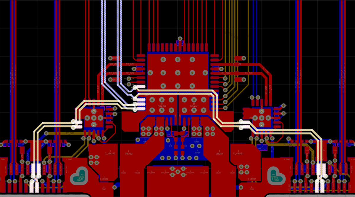
When routing the USB2 signals to the TPS65988 BC1.2 detection pins and the ESD protection to the TPS6S300 protection device, it is recommended to reduce the amount of excess trace to all of the pins. This will cause antennae and degrade signal integrity. The USB top/bottom signals are shorted together in this example and the same approach can be used if an external USB mux is used. There are several approaches that can be used to get optimal routing; “tap” the USB2 signals with vias that connect the TPS65988 pins, via up to the layer where the pins are located and continue to route on that layer, or a combination of both.
In this layout example, the D+/D- lines are routed to an internal layer from the connector. They are then via’d up to the pins on the devices. The figure below show the complete USB2 routing on SSTX1RX1, High Speed, and SSTX2RX2 layers.
 Figure 11-17 Complete USB2 Routing