SLVSDB5B July   2018  – August 2021 TPS65988

PRODUCTION DATA  

  1. Features
  2. Applications
  3. Description
  4. Revision History
  5. Pin Configuration and Functions
  6. Specifications
    1. 6.1  Absolute Maximum Ratings
    2. 6.2  ESD Ratings
    3. 6.3  Recommended Operating Conditions
    4. 6.4  Thermal Information
    5. 6.5  Power Supply Requirements and Characteristics
    6. 6.6  Power Consumption Characteristics
    7. 6.7  Power Switch Characteristics
    8. 6.8  Cable Detection Characteristics
    9. 6.9  USB-PD Baseband Signal Requirements and Characteristics
    10. 6.10 BC1.2 Characteristics
    11. 6.11 Thermal Shutdown Characteristics
    12. 6.12 Oscillator Characteristics
    13. 6.13 I/O Characteristics
    14. 6.14 PWM Driver Characteristics
    15. 6.15 I2C Requirements and Characteristics
    16. 6.16 SPI Controller Timing Requirements
    17. 6.17 HPD Timing Requirements
    18. 6.18 Typical Characteristics
  7. Parameter Measurement Information
  8. Detailed Description
    1. 8.1 Overview
    2. 8.2 Functional Block Diagram
    3. 8.3 Feature Description
      1. 8.3.1  USB-PD Physical Layer
        1. 8.3.1.1 USB-PD Encoding and Signaling
        2. 8.3.1.2 USB-PD Bi-Phase Marked Coding
        3. 8.3.1.3 USB-PD Transmit (TX) and Receive (Rx) Masks
        4. 8.3.1.4 USB-PD BMC Transmitter
        5. 8.3.1.5 USB-PD BMC Receiver
      2. 8.3.2  Power Management
        1. 8.3.2.1 Power-On And Supervisory Functions
        2. 8.3.2.2 VBUS LDO
        3. 8.3.2.3 Supply Switch Over
      3. 8.3.3  Port Power Switches
        1. 8.3.3.1 PP_HV Power Switch
          1. 8.3.3.1.1 PP_HV Over Current Clamp
          2. 8.3.3.1.2 PP_HV Over Current Protection
          3. 8.3.3.1.3 PP_HV OVP and UVP
          4. 8.3.3.1.4 PP_HV Reverse Current Protection
        2. 8.3.3.2 Schottky for Current Surge Protection
        3. 8.3.3.3 PP_EXT Power Path Control
        4. 8.3.3.4 PP_CABLE Power Switch
          1. 8.3.3.4.1 PP_CABLE Over Current Protection
          2. 8.3.3.4.2 PP_CABLE Input Good Monitor
        5. 8.3.3.5 VBUS Transition to VSAFE5V
        6. 8.3.3.6 VBUS Transition to VSAFE0V
      4. 8.3.4  Cable Plug and Orientation Detection
        1. 8.3.4.1 Configured as a DFP
        2. 8.3.4.2 Configured as a UFP
        3. 8.3.4.3 Configured as a DRP
        4. 8.3.4.4 Fast Role Swap Signaling
      5. 8.3.5  Dead Battery Operation
        1. 8.3.5.1 Dead Battery Advertisement
        2. 8.3.5.2 BUSPOWER (ADCIN1)
      6. 8.3.6  Battery Charger Detection and Advertisement
        1. 8.3.6.1 BC1.2 Data Contact Detect
        2. 8.3.6.2 BC1.2 Primary and Secondary Detection
        3. 8.3.6.3 Charging Downstream Port Advertisement
        4. 8.3.6.4 Dedicated Charging Port Advertisement
        5. 8.3.6.5 2.7V Divider3 Mode Advertisement
        6. 8.3.6.6 1.2V Mode Advertisement
        7. 8.3.6.7 DCP Auto Mode Advertisement
      7. 8.3.7  ADC
      8. 8.3.8  DisplayPort HPD
      9. 8.3.9  Digital Interfaces
        1. 8.3.9.1 General GPIO
        2. 8.3.9.2 I2C
        3. 8.3.9.3 SPI
      10. 8.3.10 PWM Driver
      11. 8.3.11 Digital Core
      12. 8.3.12 I2C Interfaces
        1. 8.3.12.1 I2C Interface Description
        2. 8.3.12.2 I2C Clock Stretching
        3. 8.3.12.3 I2C Address Setting
        4. 8.3.12.4 Unique Address Interface
        5. 8.3.12.5 I2C Pin Address Setting (ADCIN2)
      13. 8.3.13 SPI Controller Interface
      14. 8.3.14 Thermal Shutdown
      15. 8.3.15 Oscillators
    4. 8.4 Device Functional Modes
      1. 8.4.1 Boot
      2. 8.4.2 Power States
  9. Application and Implementation
    1. 9.1 Application Information
    2. 9.2 Typical Applications
      1. 9.2.1 Type-C VBUS Design Considerations
        1. 9.2.1.1 Design Requirements
        2. 9.2.1.2 Detailed Design Procedure
          1. 9.2.1.2.1 External Sink Power Path Options
            1. 9.2.1.2.1.1 Load Switch Power Path
            2. 9.2.1.2.1.2 Discrete Power Path
          2. 9.2.1.2.2 Type-C Connector VBUS Capacitors
          3. 9.2.1.2.3 VBUS Schottky and TVS Diodes
          4. 9.2.1.2.4 VBUS Snubber Circuit
        3. 9.2.1.3 Application Curves
      2. 9.2.2 Dual Port Thunderbolt Notebook with AR Supporting USB PD Charging
        1. 9.2.2.1 Design Requirements
        2. 9.2.2.2 USB Power Delivery Source Capabilities
        3. 9.2.2.3 USB Power Delivery Sink Capabilities
        4. 9.2.2.4 Supported Data Modes
        5. 9.2.2.5 RESETN
        6. 9.2.2.6 I2C Design Requirements
        7. 9.2.2.7 TS3DS10224 SBU Mux for AUX and LSTX/RX
        8. 9.2.2.8 Thunderbolt Flash Options
      3. 9.2.3 Dual Port USB & Displayport Notebook Supporting PD Charging
        1. 9.2.3.1 Design Requirements
        2. 9.2.3.2 USB Power Delivery Source Capabilities
        3. 9.2.3.3 USB Power Delivery Sink Capabilities
        4. 9.2.3.4 Supported Data Modes
        5. 9.2.3.5 TUSB1044 Re-Driver GPIO Control
      4. 9.2.4 USB Type-C & PD Monitor/Dock
        1. 9.2.4.1 Design Requirements
        2. 9.2.4.2 Detailed Design Procedure
          1. 9.2.4.2.1 USB Power Delivery Source Capabilities
          2. 9.2.4.2.2 USB and DisplayPort Supported Data Modes
          3. 9.2.4.2.3 TUSB1064 Super Speed Mux GPIO Control
  10. 10Power Supply Recommendations
    1. 10.1 3.3-V Power
      1. 10.1.1 VIN_3V3 Input Switch
      2. 10.1.2 VBUS 3.3-V LDO
    2. 10.2 1.8-V Power
    3. 10.3 Recommended Supply Load Capacitance
  11. 11Layout
    1. 11.1  Layout Guidelines
    2. 11.2  Layout Example
    3. 11.3  Stack-Up and Design Rules
    4. 11.4  Main Component Placement
    5. 11.5  1.4 Super Speed Type-C Connectors
    6. 11.6  Capacitor Placement
    7. 11.7  CC1/2 Capacitors & ADCIN1/2 Resistors
    8. 11.8  CC & SBU Protection Placement
    9. 11.9  CC Routing
    10. 11.10 DRAIN1 and DRAIN2 Pad Pours
    11. 11.11 USB2 Routing for ESD Protection and BC1.2
    12. 11.12 VBUS Routing
    13. 11.13 Completed Layout
    14. 11.14 Power Dissipation
  12. 12Device and Documentation Support
    1. 12.1 Device Support
      1. 12.1.1 Third-Party Products Disclaimer
      2. 12.1.2 Firmware Warranty Disclaimer
    2. 12.2 Receiving Notification of Documentation Updates
    3. 12.3 Support Resources
    4. 12.4 Trademarks
    5. 12.5 Electrostatic Discharge Caution
    6. 12.6 Glossary
  13. 13Mechanical, Packaging, and Orderable Information

Package Options

Mechanical Data (Package|Pins)
Thermal pad, mechanical data (Package|Pins)
Orderable Information
VBUS Snubber Circuit
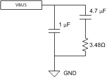
GUID-802CF983-35CB-4D98-B417-5DEEAA095EAD-low.gifFigure 9-4 VBUS Snubber

Another method of clamping the USB Type-C VBUS is to use a VBUS RC Snubber. An RC Snubber is a great solution because in general it is much smaller than a TVS diode, and typically more cost effective as well. An RC Snubber works by modifying the characteristic of the total RLC response in the USB Type-C cable hot-plug from being under-damped to critically-damped or over-damped. So rather than clamping the over-voltage directly, it actually changes the hot-plug response from under-damped to critically-damped, so the voltage on VBUS does not ring at all; so the voltage is limited, but without requiring a clamping element like a TVS diode.

However, the USB Type-C and Power Delivery specifications limit the range of capacitance that can be used on VBUS for the RC snubber. VBUS capacitance must have a minimum 1 µF and a maximum of 10 µF. The RC snubber values chosen support up to 4 m USB Type-C cable (maximum length allowed in the USB Type-C specification) being hot plugged, is to use 4.7-μF capacitor in series with a 3.48-Ω resistor. In parallel with the RC Snubber a 1 μF capacitor is used, which always ensures the minimum USB Type-C VBUS capacitance specification is met. This circuit can be seen in Figure 9-4.