SLVSFN9A September   2020  – August 2021 TPS65988DK

PRODUCTION DATA  

  1. Features
  2. Applications
  3. Description
  4. Revision History
  5. Pin Configuration and Functions
  6. Specifications
    1. 6.1  Absolute Maximum Ratings
    2. 6.2  ESD Ratings
    3. 6.3  Recommended Operating Conditions
    4. 6.4  Thermal Information
    5. 6.5  Power Supply Requirements and Characteristics
    6. 6.6  Power Consumption Characteristics
    7. 6.7  Power Switch Characteristics
    8. 6.8  Cable Detection Characteristics
    9. 6.9  USB-PD Baseband Signal Requirements and Characteristics
    10. 6.10 Thermal Shutdown Characteristics
    11. 6.11 Oscillator Characteristics
    12. 6.12 I/O Characteristics
    13. 6.13 I2C Requirements and Characteristics
    14. 6.14 SPI Controller Timing Requirements
    15. 6.15 HPD Timing Requirements
    16. 6.16 Typical Characteristics
  7. Parameter Measurement Information
  8. Detailed Description
    1. 8.1 Overview
    2. 8.2 Functional Block Diagram
    3. 8.3 Feature Description
      1. 8.3.1  USB-PD Physical Layer
        1. 8.3.1.1 USB-PD Encoding and Signaling
        2. 8.3.1.2 USB-PD Bi-Phase Marked Coding
        3. 8.3.1.3 USB-PD Transmit (TX) and Receive (Rx) Masks
        4. 8.3.1.4 USB-PD BMC Transmitter
        5. 8.3.1.5 USB-PD BMC Receiver
      2. 8.3.2  Power Management
        1. 8.3.2.1 Power-On and Supervisory Functions
        2. 8.3.2.2 VBUS LDO
        3. 8.3.2.3 Supply Switch Over
      3. 8.3.3  Port Power Switches
        1. 8.3.3.1 PP_HV Power Switch
          1. 8.3.3.1.1 PP_HV Overcurrent Clamp
          2. 8.3.3.1.2 PP_HV Overcurrent Protection
          3. 8.3.3.1.3 PP_HV OVP and UVP
          4. 8.3.3.1.4 PP_HV Reverse Current Protection
        2. 8.3.3.2 Schottky for Current Surge Protection
        3. 8.3.3.3 PP_EXT Power Path Control
        4. 8.3.3.4 PP_CABLE Power Switch
          1. 8.3.3.4.1 PP_CABLE Overcurrent Protection
          2. 8.3.3.4.2 PP_CABLE Input Good Monitor
        5. 8.3.3.5 VBUS Transition to VSAFE5V
        6. 8.3.3.6 VBUS Transition to VSAFE0V
      4. 8.3.4  Cable Plug and Orientation Detection
        1. 8.3.4.1 Configured as a DFP
        2. 8.3.4.2 Configured as a UFP
        3. 8.3.4.3 Configured as a DRP
        4. 8.3.4.4 Fast Role Swap Signaling
      5. 8.3.5  Dead Battery Operation
        1. 8.3.5.1 Dead Battery Advertisement
        2. 8.3.5.2 BUSPOWER (ADCIN1)
      6. 8.3.6  ADC
      7. 8.3.7  DisplayPort HPD
      8. 8.3.8  Digital Interfaces
        1. 8.3.8.1 General GPIO
        2. 8.3.8.2 I2C
        3. 8.3.8.3 SPI
      9. 8.3.9  Digital Core
      10. 8.3.10 I2C Interfaces
        1. 8.3.10.1 I2C Interface Description
        2. 8.3.10.2 I2C Clock Stretching
        3. 8.3.10.3 I2C Address Setting
        4. 8.3.10.4 Unique Address Interface
        5. 8.3.10.5 I2C Pin Address Setting (ADCIN2)
      11. 8.3.11 SPI Controller Interface
      12. 8.3.12 Thermal Shutdown
      13. 8.3.13 Oscillators
    4. 8.4 Device Functional Modes
      1. 8.4.1 Boot
      2. 8.4.2 Power States
  9. Application and Implementation
    1. 9.1 Application Information
    2. 9.2 Typical Applications
      1. 9.2.1 USB4 Device Application with Host Charging
        1. 9.2.1.1 Design Requirements
          1. 9.2.1.1.1 Power Supply Design Requirements
        2. 9.2.1.2 Detailed Design Procedure
          1. 9.2.1.2.1 USB Power Delivery Source Capabilities
          2. 9.2.1.2.2 USB Power Delivery Sink Capabilities
          3. 9.2.1.2.3 Supported Data Modes
          4. 9.2.1.2.4 USB4 Hub Controller & PD Controller I2C Communication
          5. 9.2.1.2.5 Dock Management Controller & PD Controller I2C Communication
          6. 9.2.1.2.6 SPI Flash Options
  10. 10Power Supply Recommendations
    1. 10.1 3.3-V Power
      1. 10.1.1 VIN_3V3 Input Switch
      2. 10.1.2 VBUS 3.3-V LDO
    2. 10.2 1.8-V Power
    3. 10.3 Recommended Supply Load Capacitance
  11. 11Layout
    1. 11.1  Layout Guidelines
    2. 11.2  Layout Example
    3. 11.3  Stack-up and Design Rules
    4. 11.4  Main Component Placement
    5. 11.5  Super Speed Type-C Connectors
    6. 11.6  Capacitor Placement
    7. 11.7  CC1/2 Capacitors & ADCIN1/2 Resistors
    8. 11.8  CC and SBU Protection Placement
    9. 11.9  CC Routing
    10. 11.10 DRAIN1 and DRAIN2 Pad Pours
    11. 11.11 VBUS Routing
    12. 11.12 Completed Layout
    13. 11.13 Power Dissipation
  12. 12Device and Documentation Support
    1. 12.1 Device Support
      1. 12.1.1 Firmware Warranty Disclaimer
    2. 12.2 Documentation Support
      1. 12.2.1 Related Documentation
    3. 12.3 Support Resources
    4. 12.4 Trademarks
    5. 12.5 Electrostatic Discharge Caution
    6. 12.6 Glossary
  13. 13Mechanical, Packaging, and Orderable Information

Package Options

Mechanical Data (Package|Pins)
Thermal pad, mechanical data (Package|Pins)
Orderable Information

I2C

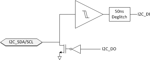
The TPS65988DK features three I2C interfaces. The I2C1 interface is configurable to operate as a master or slave. The I2C2 interface may only operate as a slave. The I2C3 interface may only operate as a master. The I2C I/O driver is shown in Figure 8-19. This I/O consists of an open-drain output and in input comparator with de-glitching. The I2C input thresholds are set by LDO_1V8 and by default.
GUID-DD8D3711-8474-4C2D-AF29-269067B740D2-low.gifFigure 8-19 I2C Buffer