SLVSFN9A September 2020 – August 2021 TPS65988DK
PRODUCTION DATA
- 1 Features
- 2 Applications
- 3 Description
- 4 Revision History
- 5 Pin Configuration and Functions
-
6 Specifications
- 6.1 Absolute Maximum Ratings
- 6.2 ESD Ratings
- 6.3 Recommended Operating Conditions
- 6.4 Thermal Information
- 6.5 Power Supply Requirements and Characteristics
- 6.6 Power Consumption Characteristics
- 6.7 Power Switch Characteristics
- 6.8 Cable Detection Characteristics
- 6.9 USB-PD Baseband Signal Requirements and Characteristics
- 6.10 Thermal Shutdown Characteristics
- 6.11 Oscillator Characteristics
- 6.12 I/O Characteristics
- 6.13 I2C Requirements and Characteristics
- 6.14 SPI Controller Timing Requirements
- 6.15 HPD Timing Requirements
- 6.16 Typical Characteristics
- 7 Parameter Measurement Information
-
8 Detailed Description
- 8.1 Overview
- 8.2 Functional Block Diagram
- 8.3
Feature Description
- 8.3.1 USB-PD Physical Layer
- 8.3.2 Power Management
- 8.3.3 Port Power Switches
- 8.3.4 Cable Plug and Orientation Detection
- 8.3.5 Dead Battery Operation
- 8.3.6 ADC
- 8.3.7 DisplayPort HPD
- 8.3.8 Digital Interfaces
- 8.3.9 Digital Core
- 8.3.10 I2C Interfaces
- 8.3.11 SPI Controller Interface
- 8.3.12 Thermal Shutdown
- 8.3.13 Oscillators
- 8.4 Device Functional Modes
- 9 Application and Implementation
- 10Power Supply Recommendations
-
11Layout
- 11.1 Layout Guidelines
- 11.2 Layout Example
- 11.3 Stack-up and Design Rules
- 11.4 Main Component Placement
- 11.5 Super Speed Type-C Connectors
- 11.6 Capacitor Placement
- 11.7 CC1/2 Capacitors & ADCIN1/2 Resistors
- 11.8 CC and SBU Protection Placement
- 11.9 CC Routing
- 11.10 DRAIN1 and DRAIN2 Pad Pours
- 11.11 VBUS Routing
- 11.12 Completed Layout
- 11.13 Power Dissipation
- 12Device and Documentation Support
- 13Mechanical, Packaging, and Orderable Information
Package Options
Mechanical Data (Package|Pins)
- RSH|56
Thermal pad, mechanical data (Package|Pins)
- RSH|56
Orderable Information
11.3 Stack-up and Design Rules
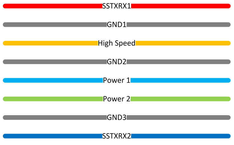
An 8-layer stack-up is used and this particular stack is common with most processor chipset guides. In some systems a 10-layer stack-up is used, the same principles can be carried over from the 8-layer to a 10-layer stack-up. Figure 11-3 shows the details of each of the layers. The two outer layers have a thickness of 1.0-oz copper and the inner layers are 0.5-oz copper.
 Figure 11-3 8 Layer Board Stack Up
Table 11-1 shows the recommended routing for each of these layers. For power routing the Power 1/2 planes can be stacked to allow for high currents.
| Layer | Routing |
|---|---|
| SSTXRX1 | Differential: 85 Z, 90 Z, 100 Z, Single Ended: 50 Z, Power, and GPIO |
| High Speed | Differential: 85 Z, 90 Z, 100 Z, Single Ended: 50 Z, and GPIO |
| Power 1 | Power and GPIO |
| Power 2 | Power and GPIO |
| SSTXRX2 | Differential: 85 Z, 90 Z, 100 Z, Single Ended: 50 Z, Power, and GPIO |
The vias used in this layout example are 8mil/16mil. There are no blind and buried vias used in this layout example and for any via on pad used it is recommended to use epoxy filled vias. The figure below shows the via sizing.
 Figure 11-4 Recommended Minimum Via Sizing