SLVSFN9A September 2020 – August 2021 TPS65988DK
PRODUCTION DATA
- 1 Features
- 2 Applications
- 3 Description
- 4 Revision History
- 5 Pin Configuration and Functions
-
6 Specifications
- 6.1 Absolute Maximum Ratings
- 6.2 ESD Ratings
- 6.3 Recommended Operating Conditions
- 6.4 Thermal Information
- 6.5 Power Supply Requirements and Characteristics
- 6.6 Power Consumption Characteristics
- 6.7 Power Switch Characteristics
- 6.8 Cable Detection Characteristics
- 6.9 USB-PD Baseband Signal Requirements and Characteristics
- 6.10 Thermal Shutdown Characteristics
- 6.11 Oscillator Characteristics
- 6.12 I/O Characteristics
- 6.13 I2C Requirements and Characteristics
- 6.14 SPI Controller Timing Requirements
- 6.15 HPD Timing Requirements
- 6.16 Typical Characteristics
- 7 Parameter Measurement Information
-
8 Detailed Description
- 8.1 Overview
- 8.2 Functional Block Diagram
- 8.3
Feature Description
- 8.3.1 USB-PD Physical Layer
- 8.3.2 Power Management
- 8.3.3 Port Power Switches
- 8.3.4 Cable Plug and Orientation Detection
- 8.3.5 Dead Battery Operation
- 8.3.6 ADC
- 8.3.7 DisplayPort HPD
- 8.3.8 Digital Interfaces
- 8.3.9 Digital Core
- 8.3.10 I2C Interfaces
- 8.3.11 SPI Controller Interface
- 8.3.12 Thermal Shutdown
- 8.3.13 Oscillators
- 8.4 Device Functional Modes
- 9 Application and Implementation
- 10Power Supply Recommendations
-
11Layout
- 11.1 Layout Guidelines
- 11.2 Layout Example
- 11.3 Stack-up and Design Rules
- 11.4 Main Component Placement
- 11.5 Super Speed Type-C Connectors
- 11.6 Capacitor Placement
- 11.7 CC1/2 Capacitors & ADCIN1/2 Resistors
- 11.8 CC and SBU Protection Placement
- 11.9 CC Routing
- 11.10 DRAIN1 and DRAIN2 Pad Pours
- 11.11 VBUS Routing
- 11.12 Completed Layout
- 11.13 Power Dissipation
- 12Device and Documentation Support
- 13Mechanical, Packaging, and Orderable Information
Package Options
Mechanical Data (Package|Pins)
- RSH|56
Thermal pad, mechanical data (Package|Pins)
- RSH|56
Orderable Information
11.6 Capacitor Placement
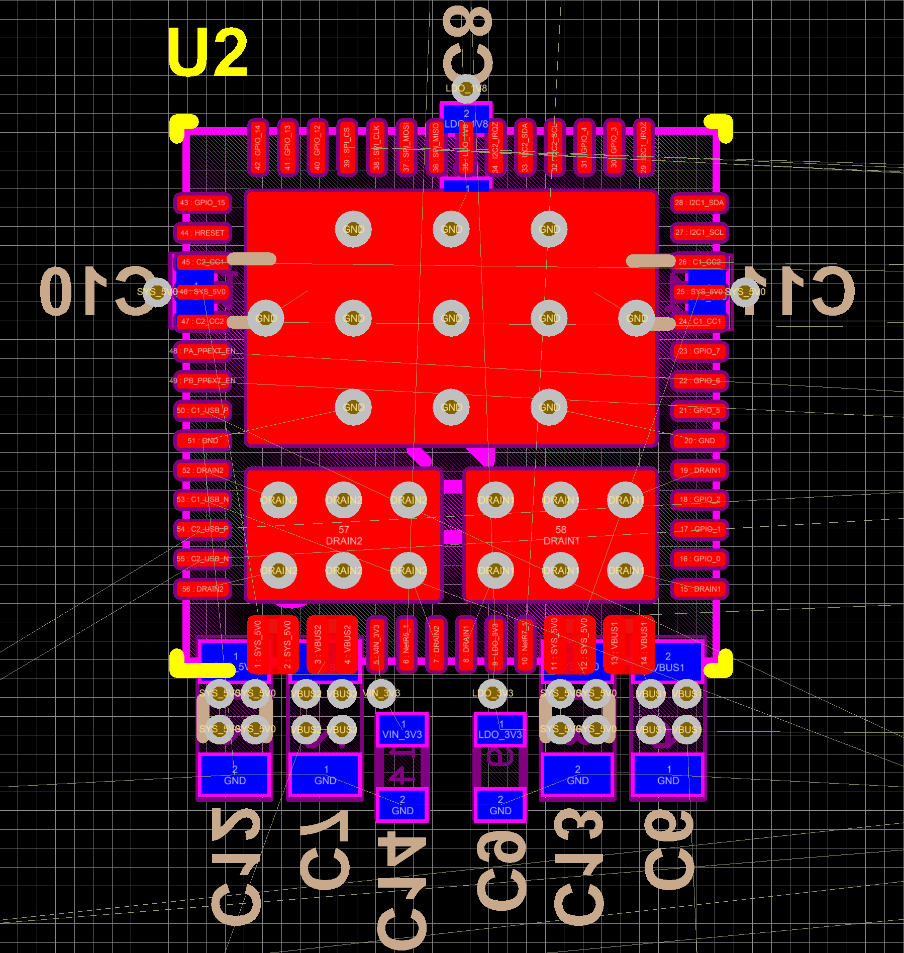
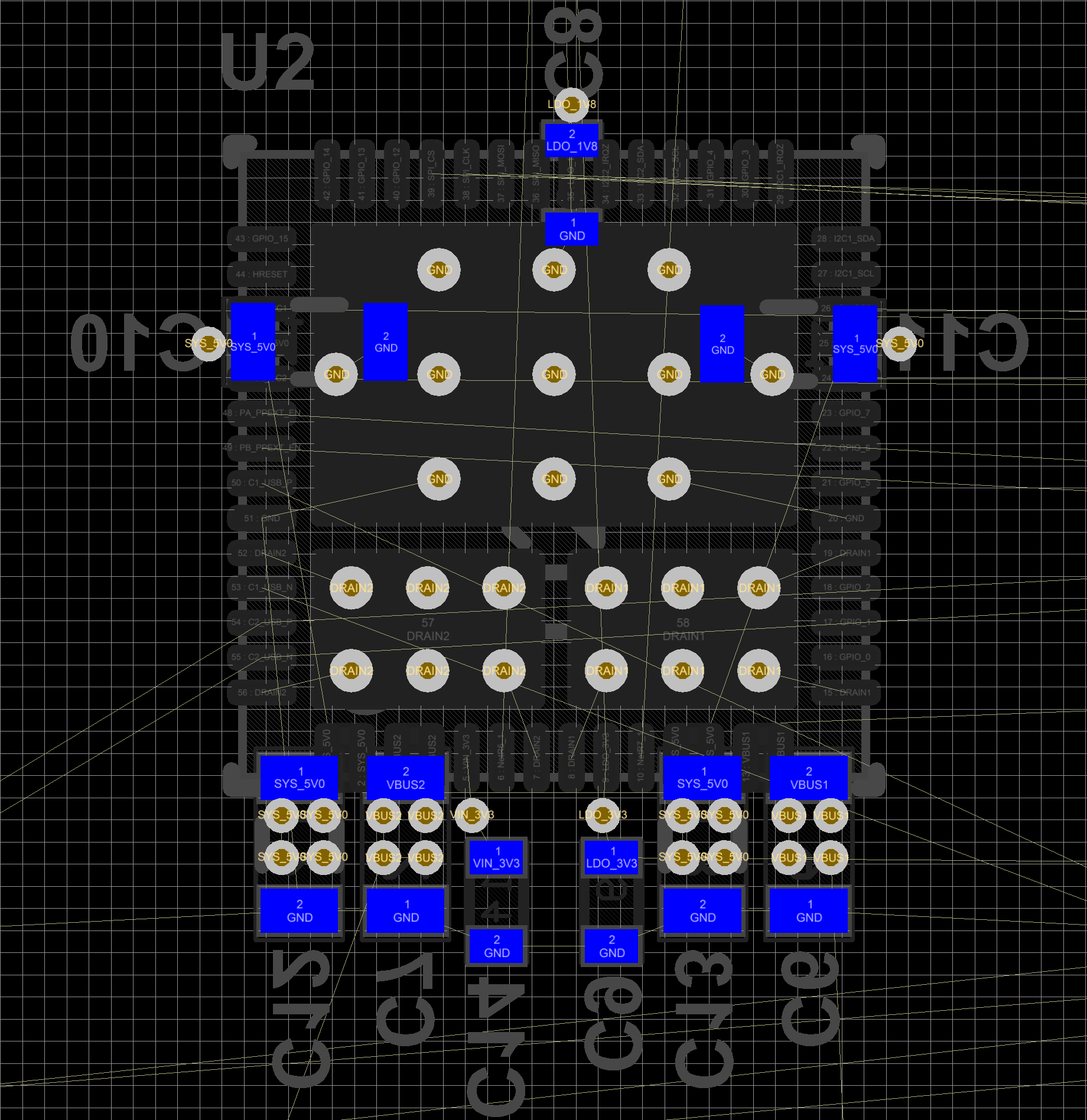
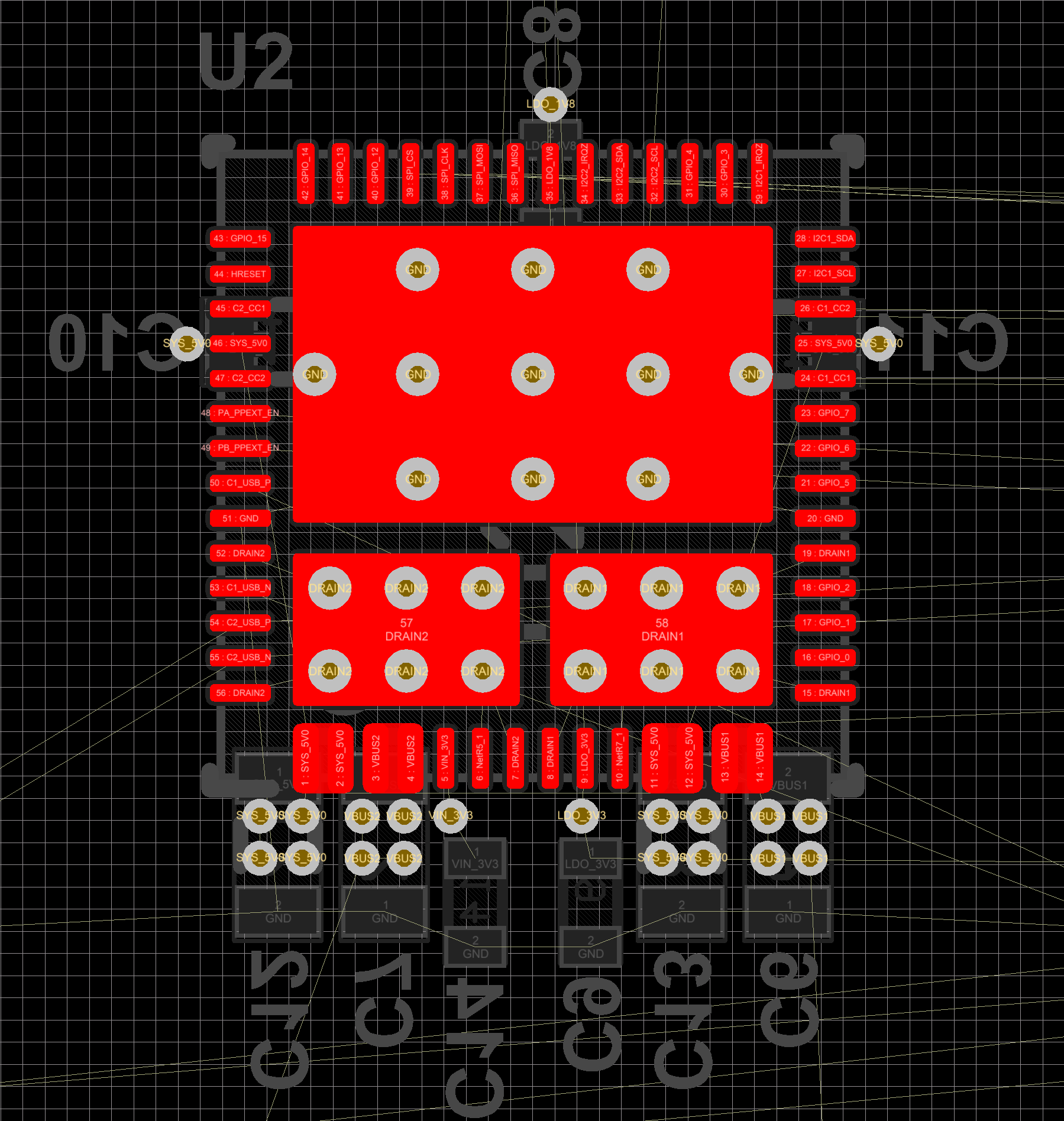
All of the capacitors for the TPS65988DK must be placed close to their respective pin. For the PP_HV1/2, VBUS1/2, VIN_3V3 and LDO_3V3 it is recommended to place their capacitors on the opposite side of the TPS65988DK with the GND terminal facing away from the TPS65988DK. This method will have all of the GND terminals together in order to have a solid plane that can be stitched to GND. The DRAIN1/2 pad will also have more room for their bottom side pour. PP_CABLE1/2 and LDO_1V8 are placed on the opposite side but their GND terminals are facing toward the TPS65988DK to share the common GND pour from the TPS65988DK GND pad. VBUS1/2 and PP_HV1/2 should have at least four vias to connect the TPS65988DK pin, capacitors and pours. For VIN_3V3, LDO_3V3, LDO_1V8 and PP_CABLE1/2 they can be connected with a single via to their capacitors and pours.
 Figure 11-9 System Capacitors Placement Top/Bottom Layer
 Figure 11-11 System Capacitors Placement Bottom Layer
 Figure 11-10 System Capacitors Placement Top Layer