SLVSFN9A September 2020 – August 2021 TPS65988DK
PRODUCTION DATA
- 1 Features
- 2 Applications
- 3 Description
- 4 Revision History
- 5 Pin Configuration and Functions
-
6 Specifications
- 6.1 Absolute Maximum Ratings
- 6.2 ESD Ratings
- 6.3 Recommended Operating Conditions
- 6.4 Thermal Information
- 6.5 Power Supply Requirements and Characteristics
- 6.6 Power Consumption Characteristics
- 6.7 Power Switch Characteristics
- 6.8 Cable Detection Characteristics
- 6.9 USB-PD Baseband Signal Requirements and Characteristics
- 6.10 Thermal Shutdown Characteristics
- 6.11 Oscillator Characteristics
- 6.12 I/O Characteristics
- 6.13 I2C Requirements and Characteristics
- 6.14 SPI Controller Timing Requirements
- 6.15 HPD Timing Requirements
- 6.16 Typical Characteristics
- 7 Parameter Measurement Information
-
8 Detailed Description
- 8.1 Overview
- 8.2 Functional Block Diagram
- 8.3
Feature Description
- 8.3.1 USB-PD Physical Layer
- 8.3.2 Power Management
- 8.3.3 Port Power Switches
- 8.3.4 Cable Plug and Orientation Detection
- 8.3.5 Dead Battery Operation
- 8.3.6 ADC
- 8.3.7 DisplayPort HPD
- 8.3.8 Digital Interfaces
- 8.3.9 Digital Core
- 8.3.10 I2C Interfaces
- 8.3.11 SPI Controller Interface
- 8.3.12 Thermal Shutdown
- 8.3.13 Oscillators
- 8.4 Device Functional Modes
- 9 Application and Implementation
- 10Power Supply Recommendations
-
11Layout
- 11.1 Layout Guidelines
- 11.2 Layout Example
- 11.3 Stack-up and Design Rules
- 11.4 Main Component Placement
- 11.5 Super Speed Type-C Connectors
- 11.6 Capacitor Placement
- 11.7 CC1/2 Capacitors & ADCIN1/2 Resistors
- 11.8 CC and SBU Protection Placement
- 11.9 CC Routing
- 11.10 DRAIN1 and DRAIN2 Pad Pours
- 11.11 VBUS Routing
- 11.12 Completed Layout
- 11.13 Power Dissipation
- 12Device and Documentation Support
- 13Mechanical, Packaging, and Orderable Information
Package Options
Mechanical Data (Package|Pins)
- RSH|56
Thermal pad, mechanical data (Package|Pins)
- RSH|56
Orderable Information
9.2.1 USB4 Device Application with Host Charging
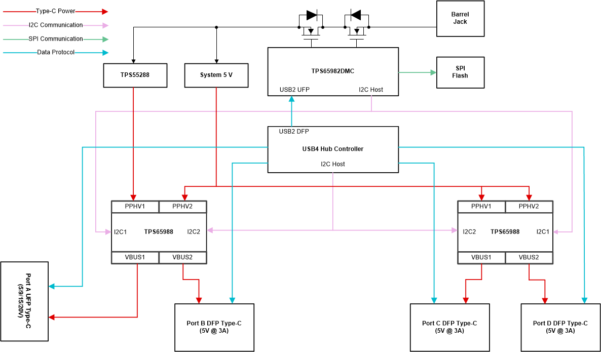
The figure below shows a USB4 Device application, where there are a total of four Type-C PD Ports. One port is the main connection to a USB4 Host that is a UFP in terms of data and a source of power. The other three ports are DFPs in terms of data and source power. Generally the main UFP source Type-C PD port provides the highest power (up to 100 W) to charge a USB4 Host. The key four devices in the system are the PD Controller (2), Dock Management Controller, USB4 Hub Controller, and UFP Variable Power Supply.
 Figure 9-1 USB4 Device Block Diagram
In this application, two dual port TPS65988DK PD controllers are used to determine the connection and provide power on the Type-C ports. The primary TPS65988DK manages Port A (UFP Source) and Port B (DFP Source). The secondary TPS65988DK manages the other two, Port C (DFP Source) and Port D (DFP Source). For systems that do not need all four ports a combination of TPS65988DK and TPS65988DK may be used to scale for specific design requirements. The PD controllers have two I2C clients that are controlled by the Dock Management Controller and the USB4 Hub Controller. The PD controllers have an optional I2C Host that may be used to control a variable power supply.
The Dock Management Controller (DMC), TPS65982DMC, main functions are the Connection Manager, Power Manager, Input Power Control, Secure Firmware Update & booting of the PD controllers. The Connection Manager determines the capabilities of the UFP connection and sets the DFP capabilities accordingly. The Power Manager keeps the power allocated to each of the Type-C ports within a specific power budget and also monitors the entire system power to keep from over loading the Barrel Jack adapter supply. The DMC also controls the input power to the system and soft starts the power path to prevent large inrush currents when the Barrel Jack supply is connected. The Secure Firmware Update is accomplished over USB2, the DMC is connected to one of the USB2 DFP ports on the USB4 Hub Controller or USB2 Hub in the system. The DMC provides the Secure Firmware Update for itself and the PD controllers. The DMC will boot the PD controllers over the I2C connection. The I2C connection between the DMC and PD controllers also serves as communication channel for the Connection and Power Manager.
The USB4 Hub Controller manages the data paths for all of the Type-C ports and determines the required data protocol by reading the PD controller status over I2C connection. The UFP port is the main connection to the USB4 Hub Controller from a USB4 host. The other DFP ports act as expansion ports to connect other USB Type-C & PD devices.
The UFP Variable Power Supply provides 5 V/9 V/15 V/20 V up to 100 W to charge the connected USB4 host. The TPS55288 is used in this application since it is capable of tightly regulating the output voltage and current. The TPS55288 is best connected to the I2C Host on the Primary PD controller, to set the output voltage and current regulation. The other DFP ports generally support 5 V @ 3 A to connect to Type-C & PD devices.