SLVSEW8B August 2019 – December 2019 TPS66020 , TPS66021
PRODUCTION DATA.
- 1 Features
- 2 Applications
- 3 Description
- 4 Revision History
- 5 Pin Configuration and Functions
-
6 Specifications
- 6.1 Absolute Maximum Ratings
- 6.2 ESD Ratings
- 6.3 Recommended Operating Conditions
- 6.4 Recommended Supply Load Capacitance
- 6.5 Thermal Information
- 6.6 PP5V Power Switch Characteristics
- 6.7 PPHV Power Switch Characteristics
- 6.8 Power Path Supervisory
- 6.9 VBUS LDO Characteristics
- 6.10 Thermal Shutdown Characteristics
- 6.11 Input-output (I/O) Characteristics
- 6.12 Power Consumption Characteristics
- 6.13 Typical Characteristics
- 7 Parameter Measurement Information
-
8 Detailed Description
- 8.1 Overview
- 8.2 Functional Block Diagram
- 8.3 Feature Description
- 8.4 Device Functional Modes
-
9 Application and Implementation
- 9.1 Application Information
- 9.2
Typical Application
- 9.2.1 Design Requirements
- 9.2.2
Detailed Design Procedure
- 9.2.2.1 External Current Reference Resistor (RIREF)
- 9.2.2.2 External VLDO Capacitor (CVLDO)
- 9.2.2.3 PP5V Power Path Capacitance
- 9.2.2.4 PPHV, VBUS Power Path Capacitance
- 9.2.2.5 VBUS TVS Protection (Optional)
- 9.2.2.6 VBUS Schottky Diode Protection (Optional)
- 9.2.2.7 VBUS Overvoltage Protection (Optional)
- 9.2.2.8 Dead Battery Support
- 9.2.2.9 Fast Role Swap (FRS) (Optional)
- 9.2.3 Application Curves
- 10Power Supply Recommendations
- 11Layout
- 12Device and Documentation Support
- 13Mechanical, Packaging, and Orderable Information
Package Options
Mechanical Data (Package|Pins)
- YBG|28
Thermal pad, mechanical data (Package|Pins)
Orderable Information
8.4.7.3 Fast Role Swap Sequence
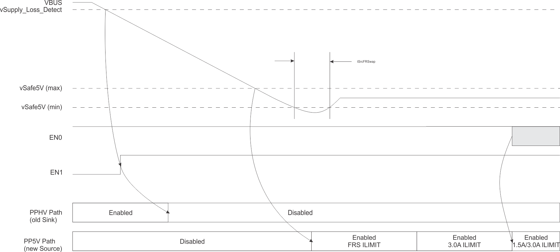
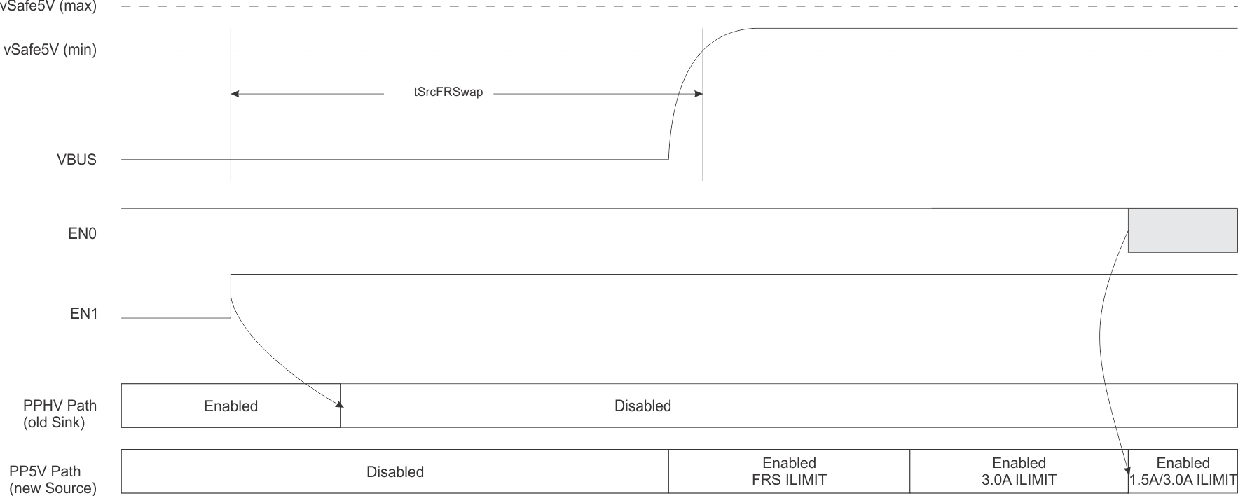
The TPS6602x supports specialized hardware to minimize unnecessary delays upon a Fast Role Swap event. Figure 25 shows the fast role swap sequencing.
- At some point, the Hub device connected to the Host detects a power loss condition and begins to transmit fast role swap signaling on its CC line to the Host PD Controller.
- The Host PD Controller's CC detection circuitry detects fast role swap signaling applied by observing the CC line and is validated.
- Upon validating the FRS signaling, the Host PD Controller shall assert EN1 = 1 of the TPS6602x as soon as possible to initiate the power role swap. It should be noted that since the transition of the FRS is initiated by the PD Controller, it is critical that the delay from detection of the FRS signaling to the assertion of EN1 be minimized.
- Upon EN1 = 1 assertion, the TPS6602x PPHV path is disabled automatically by the fast role swap hardware.
- There are two cases to consider. In Case 1, as shown in Figure 26, VBUS begins to decay, while being continuously monitored by the vSafe5V comparator circuitry that indicates when VBUS has fallen below vSafe5V. Once this occurs, the comparator output is asserted indicating to the fast role swap hardware that it is safe to turn on the PP5V path, and the PP5V path is enabled automatically. In Case 2, as shown in Figure 27, VBUS may have fallen below vSafe5V, or even fully discharged to ground, so the comparator output may already be asserted low. If so, the PP5V path shall be immediately enabled. It should be noted in this scenario, since the VBUS capacitance has been fully discharged, a significant in-rush current will occur when the PP5V path is enabled. Application should ensure sufficient decoupling capacitance is applied on the PP5V supply or that the supply is designed to react to fast transient responses to avoid brown-out of the supply rail.
- PP5V is initially enabled with a higher current limit to ensure fast turn-on. Once fast role swap is completed, it reverts back to the 3-A setting. The application may then choose to stay at the 3-A setting or switch to the 1.5-A setting.
 Figure 25. Fast Role Swap Timing
  Figure 26. Fast Role Swap Events - Case 1
  Figure 27. Fast Role Swap Events - Case 2